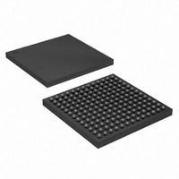
EP4CGX15BF14C8N Altera, EP4CGX15BF14C8N Datasheet - Page 321

EP4CGX15BF14C8N
Manufacturer Part Number
EP4CGX15BF14C8N
Description
IC CYCLONE IV FPGA 15K 169FBGA
Manufacturer
Altera
Series
CYCLONE® IV GXr
Datasheets
1.EP4CGX15BN11C8N.pdf
(44 pages)
2.EP4CGX15BN11C8N.pdf
(14 pages)
3.EP4CGX15BN11C8N.pdf
(478 pages)
4.EP4CGX15BN11C8N.pdf
(10 pages)
Specifications of EP4CGX15BF14C8N
Number Of Logic Elements/cells
14400
Number Of Labs/clbs
900
Total Ram Bits
540000
Number Of I /o
72
Voltage - Supply
1.16 V ~ 1.24 V
Mounting Type
Surface Mount
Operating Temperature
0°C ~ 85°C
Package / Case
169-FBGA
Lead Free Status / RoHS Status
Lead free / RoHS Compliant
Number Of Gates
-
Other names
544-1475
Available stocks
Company
Part Number
Manufacturer
Quantity
Price
Company:
Part Number:
EP4CGX15BF14C8N
Manufacturer:
ALTERA33
Quantity:
276
- EP4CGX15BN11C8N PDF datasheet
- EP4CGX15BN11C8N PDF datasheet #2
- EP4CGX15BN11C8N PDF datasheet #3
- EP4CGX15BN11C8N PDF datasheet #4
- Current page: 321 of 478
- Download datasheet (13Mb)
Chapter 1: Cyclone IV Transceivers Architecture
Calibration Block
Calibration Block
© December 2010 Altera Corporation
This block calibrates the OCT resistors and the analog portions of the transceiver
blocks to ensure that the functionality is independent of process, voltage, and
temperature (PVT) variations.
Figure 1–40
transceiver blocks.
Figure 1–40. Transceiver Calibration Blocks Location and Connection
Note to
(1) Transceiver block GXBL1 is only available for devices in F484 and larger packages.
The calibration block internally generates a constant internal reference voltage,
independent of PVT variations and uses this voltage and the external reference
resistor on the RREF pin to generate constant reference currents. The OCT calibration
circuit calibrates the OCT resistors present in the transceiver channels.
shows the calibration block diagram.
Figure 1–41. Input Signals to the Calibration Blocks
Notes to
(1) All transceiver channels use the same calibration block clock and power down signals.
(2) Connect a 2 k (tolerance max ± 1%) external resistor to the RREF pin to ground. The RREF resistor connection in
(3) Supports up to 125 MHz clock frequency. Use either dedicated global clock or divide-down logic from the FPGA fabric
(4) The calibration block restarts the calibration process following deassertion of the cal_blk_powerdown signal.
the board must be free from any external noise.
to generate a slow clock on the local clock routing.
cal_blk_powerdown (4)
Figure
OCT Calibration Control
Figure
1–40:
cal_blk_clk (3)
shows the location of the calibration block and how it is connected to the
1–41:
RREF pin (2)
2KΩ
OCT Calibration
Circuit
RREF
GXBL1 (1)
GXBL0
Calibration Block
Calibration
Block
Reference
Generator
Internal
Voltage
(Note 1)
Calibration Circuit
Cyclone IV GX
Analog Block
Device
Reference
Signal
Cyclone IV Device Handbook, Volume 2
Calibration Control
Analog Block
Figure 1–41
1–41
Related parts for EP4CGX15BF14C8N
Image
Part Number
Description
Manufacturer
Datasheet
Request
R

Part Number:
Description:
CYCLONE II STARTER KIT EP2C20N
Manufacturer:
Altera
Datasheet:

Part Number:
Description:
CPLD, EP610 Family, ECMOS Process, 300 Gates, 16 Macro Cells, 16 Reg., 16 User I/Os, 5V Supply, 35 Speed Grade, 24DIP
Manufacturer:
Altera Corporation
Datasheet:

Part Number:
Description:
CPLD, EP610 Family, ECMOS Process, 300 Gates, 16 Macro Cells, 16 Reg., 16 User I/Os, 5V Supply, 15 Speed Grade, 24DIP
Manufacturer:
Altera Corporation
Datasheet:

Part Number:
Description:
Manufacturer:
Altera Corporation
Datasheet:

Part Number:
Description:
CPLD, EP610 Family, ECMOS Process, 300 Gates, 16 Macro Cells, 16 Reg., 16 User I/Os, 5V Supply, 30 Speed Grade, 24DIP
Manufacturer:
Altera Corporation
Datasheet:

Part Number:
Description:
High-performance, low-power erasable programmable logic devices with 8 macrocells, 10ns
Manufacturer:
Altera Corporation
Datasheet:

Part Number:
Description:
High-performance, low-power erasable programmable logic devices with 8 macrocells, 7ns
Manufacturer:
Altera Corporation
Datasheet:

Part Number:
Description:
Classic EPLD
Manufacturer:
Altera Corporation
Datasheet:

Part Number:
Description:
High-performance, low-power erasable programmable logic devices with 8 macrocells, 10ns
Manufacturer:
Altera Corporation
Datasheet:

Part Number:
Description:
Manufacturer:
Altera Corporation
Datasheet:

Part Number:
Description:
Manufacturer:
Altera Corporation
Datasheet:

Part Number:
Description:
Manufacturer:
Altera Corporation
Datasheet:

Part Number:
Description:
CPLD, EP610 Family, ECMOS Process, 300 Gates, 16 Macro Cells, 16 Reg., 16 User I/Os, 5V Supply, 25 Speed Grade, 24DIP
Manufacturer:
Altera Corporation
Datasheet:


