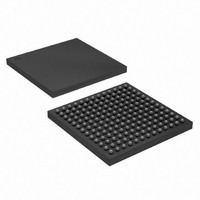
EP4CGX15BF14C8N Altera, EP4CGX15BF14C8N Datasheet - Page 151

EP4CGX15BF14C8N
Manufacturer Part Number
EP4CGX15BF14C8N
Description
IC CYCLONE IV FPGA 15K 169FBGA
Manufacturer
Altera
Series
CYCLONE® IV GXr
Datasheets
1.EP4CGX15BN11C8N.pdf
(44 pages)
2.EP4CGX15BN11C8N.pdf
(14 pages)
3.EP4CGX15BN11C8N.pdf
(478 pages)
4.EP4CGX15BN11C8N.pdf
(10 pages)
Specifications of EP4CGX15BF14C8N
Number Of Logic Elements/cells
14400
Number Of Labs/clbs
900
Total Ram Bits
540000
Number Of I /o
72
Voltage - Supply
1.16 V ~ 1.24 V
Mounting Type
Surface Mount
Operating Temperature
0°C ~ 85°C
Package / Case
169-FBGA
Lead Free Status / RoHS Status
Lead free / RoHS Compliant
Number Of Gates
-
Other names
544-1475
Available stocks
Company
Part Number
Manufacturer
Quantity
Price
Company:
Part Number:
EP4CGX15BF14C8N
Manufacturer:
ALTERA33
Quantity:
276
- EP4CGX15BN11C8N PDF datasheet
- EP4CGX15BN11C8N PDF datasheet #2
- EP4CGX15BN11C8N PDF datasheet #3
- EP4CGX15BN11C8N PDF datasheet #4
- Current page: 151 of 478
- Download datasheet (13Mb)
Chapter 7: External Memory Interfaces in Cyclone IV Devices
Cyclone IV Devices Memory Interfaces Pin Support
Table 7–1. Cyclone IV GX Device DQS and DQ Bus Mode Support for Each Side of the Device
© December 2010 Altera Corporation
EP4CGX15
EP4CGX22
EP4CGX30
EP4CGX50
EP4CGX75
Device
f
148-pin QFN
169-pin FBGA
169-pin FBGA
324-pin FBGA
484-pin FBGA
484-pin FBGA
672-pin FBGA
All I/O banks in Cyclone IV devices can support DQ and DQS signals with DQ-bus
modes of ×8, ×9, ×16, ×18, ×32, and ×36 except Cyclone IV GX devices that do not
support left I/O bank interface. DDR2 and DDR SDRAM interfaces use ×8 mode DQS
group regardless of the interface width. For a wider interface, you can use multiple ×8
DQ groups to achieve the desired width requirement.
In the ×9, ×18, and ×36 modes, a pair of complementary DQS pins (CQ and CQ#)
drives up to 9, 18, or 36 DQ pins, respectively, in the group, to support one, two, or
four parity bits and the corresponding data bits. The ×9, ×18, and ×36 modes support
the QDR II memory interface. CQ# is the inverted read-clock signal that is connected
to the complementary data strobe (DQS or CQ#) pin. You can use any unused DQ
pins as regular user I/O pins if they are not used as memory interface signals.
For more information about unsupported DQS and DQ groups of the Cyclone IV
transceivers that run at 2.97 Gbps data rate, refer to the
Connection
Table 7–1
Cyclone IV GX device.
Package
(4)
lists the number of DQS or DQ groups supported on each side of the
Guidelines.
Right
Top
Bottom
Right
Top
Bottom
Right
Top
Bottom
Right
Top
Bottom
Right
Top
Bottom
Right
Top
Bottom
Right
Top
Bottom
(2)
(2)
(2)
Side
(3)
(3)
(3)
Number
Groups
×8
1
1
1
1
1
1
1
1
1
2
2
2
4
4
4
4
4
4
4
4
4
Number
Groups
×9
0
0
0
0
0
0
0
0
0
2
2
2
2
2
2
2
2
2
2
2
2
Number
Groups
×16
0
0
0
0
0
0
0
0
0
1
1
1
2
2
2
2
2
2
2
2
2
Cyclone IV Device Family Pin
Cyclone IV Device Handbook, Volume 1
Number
Groups
(Note 1)
×18
0
0
0
0
0
0
0
0
0
1
1
1
2
2
2
2
2
2
2
2
2
Number
(Part 1 of 2)
Groups
×32
—
—
—
—
—
—
—
—
—
—
—
—
1
1
1
1
1
1
1
1
1
Number
Groups
×36
—
—
—
—
—
—
—
—
—
—
—
—
1
1
1
1
1
1
1
1
1
7–3
Related parts for EP4CGX15BF14C8N
Image
Part Number
Description
Manufacturer
Datasheet
Request
R

Part Number:
Description:
CYCLONE II STARTER KIT EP2C20N
Manufacturer:
Altera
Datasheet:

Part Number:
Description:
CPLD, EP610 Family, ECMOS Process, 300 Gates, 16 Macro Cells, 16 Reg., 16 User I/Os, 5V Supply, 35 Speed Grade, 24DIP
Manufacturer:
Altera Corporation
Datasheet:

Part Number:
Description:
CPLD, EP610 Family, ECMOS Process, 300 Gates, 16 Macro Cells, 16 Reg., 16 User I/Os, 5V Supply, 15 Speed Grade, 24DIP
Manufacturer:
Altera Corporation
Datasheet:

Part Number:
Description:
Manufacturer:
Altera Corporation
Datasheet:

Part Number:
Description:
CPLD, EP610 Family, ECMOS Process, 300 Gates, 16 Macro Cells, 16 Reg., 16 User I/Os, 5V Supply, 30 Speed Grade, 24DIP
Manufacturer:
Altera Corporation
Datasheet:

Part Number:
Description:
High-performance, low-power erasable programmable logic devices with 8 macrocells, 10ns
Manufacturer:
Altera Corporation
Datasheet:

Part Number:
Description:
High-performance, low-power erasable programmable logic devices with 8 macrocells, 7ns
Manufacturer:
Altera Corporation
Datasheet:

Part Number:
Description:
Classic EPLD
Manufacturer:
Altera Corporation
Datasheet:

Part Number:
Description:
High-performance, low-power erasable programmable logic devices with 8 macrocells, 10ns
Manufacturer:
Altera Corporation
Datasheet:

Part Number:
Description:
Manufacturer:
Altera Corporation
Datasheet:

Part Number:
Description:
Manufacturer:
Altera Corporation
Datasheet:

Part Number:
Description:
Manufacturer:
Altera Corporation
Datasheet:

Part Number:
Description:
CPLD, EP610 Family, ECMOS Process, 300 Gates, 16 Macro Cells, 16 Reg., 16 User I/Os, 5V Supply, 25 Speed Grade, 24DIP
Manufacturer:
Altera Corporation
Datasheet:


