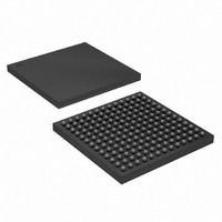
EP4CGX15BF14C8N Altera, EP4CGX15BF14C8N Datasheet - Page 30

EP4CGX15BF14C8N
Manufacturer Part Number
EP4CGX15BF14C8N
Description
IC CYCLONE IV FPGA 15K 169FBGA
Manufacturer
Altera
Series
CYCLONE® IV GXr
Datasheets
1.EP4CGX15BN11C8N.pdf
(44 pages)
2.EP4CGX15BN11C8N.pdf
(14 pages)
3.EP4CGX15BN11C8N.pdf
(478 pages)
4.EP4CGX15BN11C8N.pdf
(10 pages)
Specifications of EP4CGX15BF14C8N
Number Of Logic Elements/cells
14400
Number Of Labs/clbs
900
Total Ram Bits
540000
Number Of I /o
72
Voltage - Supply
1.16 V ~ 1.24 V
Mounting Type
Surface Mount
Operating Temperature
0°C ~ 85°C
Package / Case
169-FBGA
Lead Free Status / RoHS Status
Lead free / RoHS Compliant
Number Of Gates
-
Other names
544-1475
Available stocks
Company
Part Number
Manufacturer
Quantity
Price
Company:
Part Number:
EP4CGX15BF14C8N
Manufacturer:
ALTERA33
Quantity:
276
- EP4CGX15BN11C8N PDF datasheet
- EP4CGX15BN11C8N PDF datasheet #2
- EP4CGX15BN11C8N PDF datasheet #3
- EP4CGX15BN11C8N PDF datasheet #4
- Current page: 30 of 478
- Download datasheet (13Mb)
2–2
Figure 2–1. Cyclone IV Device LEs
LE Features
Cyclone IV Device Handbook, Volume 1
data 1
data 2
data 3
data 4
Figure 2–1
You can configure the programmable register of each LE for D, T, JK, or SR flipflop
operation. Each register has data, clock, clock enable, and clear inputs. Signals that
use the global clock network, general-purpose I/O pins, or any internal logic can
drive the clock and clear control signals of the register. Either general-purpose I/O
pins or the internal logic can drive the clock enable. For combinational functions, the
LUT output bypasses the register and drives directly to the LE outputs.
Each LE has three outputs that drive the local, row, and column routing resources.
The LUT or register output independently drives these three outputs. Two LE outputs
drive the column or row and direct link routing connections, while one LE drives the
local interconnect resources. This allows the LUT to drive one output while the
register drives another output. This feature, called register packing, improves device
utilization because the device can use the register and the LUT for unrelated
functions. The LAB-wide synchronous load control signal is not available when using
register packing. For more information about the synchronous load control signal,
refer to
The register feedback mode allows the register output to feed back into the LUT of the
same LE to ensure that the register is packed with its own fan-out LUT, providing
another mechanism for improved fitting. The LE can also drive out registered and
unregistered versions of the LUT output.
Register Feedback
LE Carry-In
Look-Up Table
“LAB Control Signals” on page
(LUT)
shows the LEs for Cyclone IV devices.
LE Carry-Out
Register Chain
Chain
Routing from
Carry
previous LE
(DEV_CLRn)
Chip-Wide
labclkena1
labclkena2
labclr1
labclr2
Reset
labclk2
labclk1
Synchronous
LAB-Wide
Chapter 2: Logic Elements and Logic Array Blocks in Cyclone IV Devices
Load
Asynchronous
Synchronous
Clock Enable
Clear Logic
Clear Logic
Load and
Clock &
Select
Synchronous
LAB-Wide
2–6.
Clear
Register Bypass
D
ENA
CLRN
Q
© November 2009 Altera Corporation
Register Chain
Output
Row, Column,
And Direct Link
Routing
Row, Column,
And Direct Link
Routing
Local
Routing
Logic Elements
Related parts for EP4CGX15BF14C8N
Image
Part Number
Description
Manufacturer
Datasheet
Request
R

Part Number:
Description:
CYCLONE II STARTER KIT EP2C20N
Manufacturer:
Altera
Datasheet:

Part Number:
Description:
CPLD, EP610 Family, ECMOS Process, 300 Gates, 16 Macro Cells, 16 Reg., 16 User I/Os, 5V Supply, 35 Speed Grade, 24DIP
Manufacturer:
Altera Corporation
Datasheet:

Part Number:
Description:
CPLD, EP610 Family, ECMOS Process, 300 Gates, 16 Macro Cells, 16 Reg., 16 User I/Os, 5V Supply, 15 Speed Grade, 24DIP
Manufacturer:
Altera Corporation
Datasheet:

Part Number:
Description:
Manufacturer:
Altera Corporation
Datasheet:

Part Number:
Description:
CPLD, EP610 Family, ECMOS Process, 300 Gates, 16 Macro Cells, 16 Reg., 16 User I/Os, 5V Supply, 30 Speed Grade, 24DIP
Manufacturer:
Altera Corporation
Datasheet:

Part Number:
Description:
High-performance, low-power erasable programmable logic devices with 8 macrocells, 10ns
Manufacturer:
Altera Corporation
Datasheet:

Part Number:
Description:
High-performance, low-power erasable programmable logic devices with 8 macrocells, 7ns
Manufacturer:
Altera Corporation
Datasheet:

Part Number:
Description:
Classic EPLD
Manufacturer:
Altera Corporation
Datasheet:

Part Number:
Description:
High-performance, low-power erasable programmable logic devices with 8 macrocells, 10ns
Manufacturer:
Altera Corporation
Datasheet:

Part Number:
Description:
Manufacturer:
Altera Corporation
Datasheet:

Part Number:
Description:
Manufacturer:
Altera Corporation
Datasheet:

Part Number:
Description:
Manufacturer:
Altera Corporation
Datasheet:

Part Number:
Description:
CPLD, EP610 Family, ECMOS Process, 300 Gates, 16 Macro Cells, 16 Reg., 16 User I/Os, 5V Supply, 25 Speed Grade, 24DIP
Manufacturer:
Altera Corporation
Datasheet:


