MCIMX53-START Freescale Semiconductor, MCIMX53-START Datasheet - Page 45
MCIMX53-START
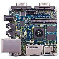
Manufacturer Part Number
MCIMX53-START
Description
KIT DEVELOPMENT I.MX53
Manufacturer
Freescale Semiconductor
Series
i.MX53r
Type
MCUr
Datasheets
1.MCIMX53-START.pdf
(2 pages)
2.MCIMX53-START.pdf
(180 pages)
3.MCIMX53-START.pdf
(204 pages)
Specifications of MCIMX53-START
Contents
Board
Silicon Manufacturer
Freescale
Core Architecture
ARM
Core Sub-architecture
Cortex - A8
Silicon Core Number
I.MX5
Silicon Family Name
I.MX53
Peak Reflow Compatible (260 C)
Yes
Rohs Compliant
Yes
Leaded Process Compatible
Yes
Lead Free Status / RoHS Status
Lead free / RoHS Compliant
For Use With/related Products
i.MX53
Lead Free Status / Rohs Status
Supplier Unconfirmed
Available stocks
Company
Part Number
Manufacturer
Quantity
Price


4.6.5
This section provides the relative timing requirements among various signals of NFC at the module level,
in each operational mode.
Timing parameters in
NFC mode (asymmetric mode) using two Flash clock cycles per one access of RE_B and WE_B.
Timing parameters in
NFC mode using one Flash clock cycle per one access of RE_B and WE_B.
With reference to the timing diagrams, a high is defined as 80% of signal value and low is defined as 20%
of signal value. All parameters are given in nanoseconds. The BGA contact load used in calculations is
20 pF (except for NF16 - 40 pF) and there is maximum drive strength on all contacts.
All timing parameters are a function of T, which is the period of the flash_clk clock (“enfc_clk” at system
level). This clock frequency can be controlled by the user, configuring CCM (SoC clock controller). The
clock is derived from emi_slow_clk after single divider.
Table 33
Freescale Semiconductor
1
2
3
4
5
Frequency lock time
(FOL mode or non-integer MF)
Phase lock time
Frequency jitter
Phase jitter (peak value)
Power dissipation
Device input range cannot exceed the electrical specifications of the CAMP, see
The values specified here are internal to DPLL. Inside the DPLL, a “1” is added to the value specified by the user. Therefore,
the user has to enter a value “1” less than the desired value at the inputs of DPLL for PDF and MFD.
The maximum total multiplication factor (MFI + MFN/MFD) allowed is 15. Therefore, if the MFI value is 15, MFN value must
be zero.
T
mode is 398 cycles of divided reference clock when DPLL starts after full reset.
Tdck is the time period of the output clock, dpdck_2.
emi_slow_clk (MHz)
dpdref
100 (Boot mode)
is the time period of the reference clock after predivider. According to the specification, the maximum lock time in FOL
demonstrates several examples of clock frequency settings.
NAND Flash Controller (NFC) Parameters
Parameter
5
(peak value)
4
i.MX53xA Automotive and Infotainment Applications Processors, Rev. 1
Figure
Figure
Table 32. DPLL Electrical Parameters (continued)
10,
10,
nfc_podf (Division Factor)
Figure
Figure
Table 33. NFC Clock Settings Examples
FPL mode, integer and fractional MF
f
dvdd = 1.2 V
f
dvdd = 1.2 V
dck
dck
= 300 MHz @ avdd = 1.8 V,
= 650 MHz @ avdd = 1.8 V,
7
11,
11,
3
Test Conditions/Remarks
1
2
Figure
Figure
12,
12,
—
—
—
Figure
Figure
13,
14,
enfc_clk (MHz)
Figure
Figure
14.29
33.33
Table
Min
15, and
15, and
—
—
—
—
—
31.
Table 34
Table 34
0.02
Typ
2.0
—
—
—
Electrical Characteristics
T-Clock Period (ns)
0.65 (avdd)
0.92 (dvdd)
1.98 (avdd)
1.8 (dvdd)
show symmetric
show the default
Max
0.04
398
100
3.5
70
30
T
Unit
d
T
mW
pdref
ns
µ
dck
s
45
Related parts for MCIMX53-START
Image
Part Number
Description
Manufacturer
Datasheet
Request
R

Part Number:
Description:
MCIMX-LVDS1
Manufacturer:
Freescale Semiconductor
Datasheet:

Part Number:
Description:
Manufacturer:
Freescale Semiconductor, Inc
Datasheet:
Part Number:
Description:
Manufacturer:
Freescale Semiconductor, Inc
Datasheet:
Part Number:
Description:
Manufacturer:
Freescale Semiconductor, Inc
Datasheet:
Part Number:
Description:
Manufacturer:
Freescale Semiconductor, Inc
Datasheet:
Part Number:
Description:
Manufacturer:
Freescale Semiconductor, Inc
Datasheet:
Part Number:
Description:
Manufacturer:
Freescale Semiconductor, Inc
Datasheet:
Part Number:
Description:
Manufacturer:
Freescale Semiconductor, Inc
Datasheet:
Part Number:
Description:
Manufacturer:
Freescale Semiconductor, Inc
Datasheet:
Part Number:
Description:
Manufacturer:
Freescale Semiconductor, Inc
Datasheet:
Part Number:
Description:
Manufacturer:
Freescale Semiconductor, Inc
Datasheet:
Part Number:
Description:
Manufacturer:
Freescale Semiconductor, Inc
Datasheet:
Part Number:
Description:
Manufacturer:
Freescale Semiconductor, Inc
Datasheet:
Part Number:
Description:
Manufacturer:
Freescale Semiconductor, Inc
Datasheet:
Part Number:
Description:
Manufacturer:
Freescale Semiconductor, Inc
Datasheet: