MCIMX53-START Freescale Semiconductor, MCIMX53-START Datasheet - Page 29
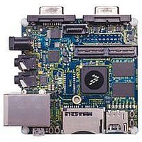
MCIMX53-START
Manufacturer Part Number
MCIMX53-START
Description
KIT DEVELOPMENT I.MX53
Manufacturer
Freescale Semiconductor
Series
i.MX53r
Type
MCUr
Datasheets
1.MCIMX53-START.pdf
(2 pages)
2.MCIMX53-START.pdf
(180 pages)
3.MCIMX53-START.pdf
(204 pages)
Specifications of MCIMX53-START
Contents
Board
Silicon Manufacturer
Freescale
Core Architecture
ARM
Core Sub-architecture
Cortex - A8
Silicon Core Number
I.MX5
Silicon Family Name
I.MX53
Peak Reflow Compatible (260 C)
Yes
Rohs Compliant
Yes
Leaded Process Compatible
Yes
Lead Free Status / RoHS Status
Lead free / RoHS Compliant
For Use With/related Products
i.MX53
Lead Free Status / Rohs Status
Supplier Unconfirmed
Available stocks
Company
Part Number
Manufacturer
Quantity
Price


1
2
3
4
4.3.2
The LPDDR2 I/O pads support DDR2/LVDDR2, LPDDR2, and DDR3 operational modes.
4.3.2.1
The DDR2 interface fully complies with JESD79-2E DDR2 JEDEC standard release April, 2008. The
parameters in
Freescale Semiconductor
Low-level output current
(1.65-3.1V OVDD)
High-Level DC input voltage
Low-Level DC input voltage
Input Hysteresis
Schmitt trigger VT+
Schmitt trigger VT–
Input current (no pull-up/down)
Input current (22 kΩ Pull-up)
Input current (47 kΩ Pull-up)
Input current (100 kΩ Pull-up)
Input current (100 kΩ Pull-down)
Keeper Circuit Resistance
Overshoot and undershoot conditions (transitions above OVDD and below GND) on switching pads must be held below 0.6 V,
and the duration of the overshoot/undershoot must not exceed 10% of the system clock cycle. Overshoot/ undershoot must be
controlled through printed circuit board layout, transmission line impedance matching, signal line termination, or other
methods. Non-compliance to this specification may affect device reliability or cause permanent damage to the device.
To maintain a valid level, the transition edge of the input must sustain a constant slew rate (monotonic) from the current DC
level through to the target DC level, VIL or VIH. Monotonic input transition time is from 0.1 ns to 1 s.
Hysteresis of 250 mV is guaranteed over all operating conditions when hysteresis is enabled.
Use an off-chip pull resistor of less than 60kΩ to override this keeper.
Parameter
LPDDR2 I/O DC Parameters
DDR2 Mode I/O DC Parameters
Table 11
2, 3
2, 3
i.MX53xA Automotive and Infotainment Applications Processors, Rev. 1
Table 10. GPIO I/O DC Electrical Characteristics (continued)
1, 2
are guaranteed per the operating ranges in
1, 2
Symbol
VHYS
VT+
VT–
VIH
VIL
IIN
IIN
IIN
IIN
IIN
Iol
Vout = 0.2
Low drive
Medium drive
High drive
Max drive
Test Conditions
OVDD = 1.875 V
OVDD = 2.775 V
VI = OVDD
VI = OVDD
VI = OVDD
V I= OVDD
VI = OVDD
VI = 0 V
VI = 0 V
VI = 0 V
VI = 0 V
VI = 0 V
×
—
—
—
—
OVDD
0.7
0.5
Table
×
×
0.25
Min
2.1
4.2
6.3
8.4
1.7
—
—
—
—
—
—
0
OVDD
OVDD
6, unless otherwise noted.
125
0.34
0.45
Typ
—
—
—
—
—
—
—
—
—
—
4
Electrical Characteristics
0.3
0.5
OVDD
×
×
Max
0.12
0.12
0.12
0.25
250
120
161
76
36
36
—
—
—
—
OVDD
OVDD
Unit
mA
nA
μA
μA
μA
μA
kΩ
V
V
V
V
V
29
Related parts for MCIMX53-START
Image
Part Number
Description
Manufacturer
Datasheet
Request
R

Part Number:
Description:
MCIMX-LVDS1
Manufacturer:
Freescale Semiconductor
Datasheet:

Part Number:
Description:
Manufacturer:
Freescale Semiconductor, Inc
Datasheet:
Part Number:
Description:
Manufacturer:
Freescale Semiconductor, Inc
Datasheet:
Part Number:
Description:
Manufacturer:
Freescale Semiconductor, Inc
Datasheet:
Part Number:
Description:
Manufacturer:
Freescale Semiconductor, Inc
Datasheet:
Part Number:
Description:
Manufacturer:
Freescale Semiconductor, Inc
Datasheet:
Part Number:
Description:
Manufacturer:
Freescale Semiconductor, Inc
Datasheet:
Part Number:
Description:
Manufacturer:
Freescale Semiconductor, Inc
Datasheet:
Part Number:
Description:
Manufacturer:
Freescale Semiconductor, Inc
Datasheet:
Part Number:
Description:
Manufacturer:
Freescale Semiconductor, Inc
Datasheet:
Part Number:
Description:
Manufacturer:
Freescale Semiconductor, Inc
Datasheet:
Part Number:
Description:
Manufacturer:
Freescale Semiconductor, Inc
Datasheet:
Part Number:
Description:
Manufacturer:
Freescale Semiconductor, Inc
Datasheet:
Part Number:
Description:
Manufacturer:
Freescale Semiconductor, Inc
Datasheet:
Part Number:
Description:
Manufacturer:
Freescale Semiconductor, Inc
Datasheet: