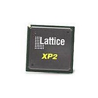
LFXP2-8E-5FTN256C Lattice, LFXP2-8E-5FTN256C Datasheet - Page 319

LFXP2-8E-5FTN256C
Manufacturer Part Number
LFXP2-8E-5FTN256C
Description
FPGA - Field Programmable Gate Array 8K LUTs 201I/O Inst- on DSP 1.2V -5 Spd
Manufacturer
Lattice
Datasheet
1.LFXP2-8E-5FTN256I.pdf
(341 pages)
Specifications of LFXP2-8E-5FTN256C
Number Of Macrocells
8000
Number Of Programmable I/os
201
Data Ram Size
226304
Supply Voltage (max)
1.26 V
Maximum Operating Temperature
+ 85 C
Minimum Operating Temperature
0 C
Mounting Style
SMD/SMT
Supply Voltage (min)
1.14 V
Package / Case
FTBGA-256
Lead Free Status / RoHS Status
Lead free / RoHS Compliant
Available stocks
Company
Part Number
Manufacturer
Quantity
Price
Company:
Part Number:
LFXP2-8E-5FTN256C
Manufacturer:
Lattice
Quantity:
63
Company:
Part Number:
LFXP2-8E-5FTN256C
Manufacturer:
Lattice Semiconductor Corporation
Quantity:
10 000
- Current page: 319 of 341
- Download datasheet (10Mb)
November 2010
Introduction
Lattice is the inventor and the leader in the (ISP) In-System Programming PLD technology. One of the visions and
ultimate goal of ISP is the live field upgrade of a mission critical system. Being a mission critical system, the field
upgrade process must meet the following criteria.
With the introduction of the LatticeXP2 Flash based non-volatile FPGA family, Lattice deliver the first and only ISP
products with all the critical attributes required to provide the ultimate solution of ISP, reliable and secure live field
upgrade of a mission critical system. The critical attributes are:
The block diagram of the LatticeXP2 device shown in Figure 17-1 provides a bird’s eye view for the unique co-exis-
tence of the Master SPI port with the Slave SPI port. The detail of the LatticeXP2 Slave SPI interface can be found
in the document dedicated on the subject. TransFR, the must have feature for the mission critical field upgrade, is
available only on the JTAG port. Therefore, the programming activities described in this document will focus on the
JTAG port only.
Figure 17-1. LatticeXP2 Master SPI and Slave SPI Ports
© 2010 Lattice Semiconductor Corp. All Lattice trademarks, registered trademarks, patents, and disclaimers are as listed at www.latticesemi.com/legal. All other brand
or product names are trademarks or registered trademarks of their respective holders. The specifications and information herein are subject to change without notice.
www.latticesemi.com
CSSPISN/IO
CSSPISN/IO
SOSPI/IO
DONE/IO
CCLK/IO
INITN/IO
SISPI/IO
1. It must be extremely reliable as any form of programming failure is not acceptable.
2. The system must remain functional throughout as even a small interruption is not acceptable including
3. Various security features will be required to protect the IP (Intellectual Property) of the mission critical sys-
1. Dual boot feature and Flash Protect to provide the extremely reliable system.
2. Instant-on, Background Programming, and TransFR features provide seamless live field upgrade.
3. Key Protect and Encryption to protect users’ Intellectual Property.
transitioning from the current pattern to the newly updated pattern.
tem.
1
0
SISPI (Read Command Out)
CCLK (Read Clock Out)
1
0
Program = 0 or Off.
Chip Select
DONE (I/O)
INITN (I/O)
Erase = 1 or On.
Persistent Fuse.
User I/O
User I/O
User I/O
User I/O
LatticeXP2
Master SPI Active
4
Engine
Slave
Master
Engine
SPI
SPI
Flash ENABLE
TAG Enable
17-1
CONFIG.
LatticeXP2 Dual Boot Feature
Configure
Firing
Circuit
3
3
Primitive
SSPIA
Primitiv
DONE Fuse State
Power Cycling
PROGRAMN (Input)
CFG1 Pin Setting
SSPIA
e
TAG Memory Flash
Embedded Flash
Oscillator
Master
Clock
User Logic
User Logic
The 4 Internal
The 4 Internal
SSPI Nodes
SSPI Nodes
User I/O
User I/O
1
0
JTAG
Technical Note TN1220
Programming
Fuse Matrix for
CFG1/IO
I/O Routing
CFG0
tn1220_01.0
TCK
TDI
TMS
TDO
User I/O
Any 4
Related parts for LFXP2-8E-5FTN256C
Image
Part Number
Description
Manufacturer
Datasheet
Request
R

Part Number:
Description:
FPGA - Field Programmable Gate Array 8K LUTs 100I/O Inst- on DSP 1.2V -5 Spd
Manufacturer:
Lattice
Datasheet:

Part Number:
Description:
FPGA - Field Programmable Gate Array 8K LUTs 201 I/O Inst on DSP 1.2V -5 Spd
Manufacturer:
Lattice
Datasheet:

Part Number:
Description:
FPGA - Field Programmable Gate Array 8K LUTs 100 I/O Inst on DSP 1.2V -5 Spd
Manufacturer:
Lattice
Datasheet:

Part Number:
Description:
IC, LATTICEXP2 FPGA, 435MHZ, QFP-208
Manufacturer:
LATTICE SEMICONDUCTOR
Datasheet:

Part Number:
Description:
FPGA - Field Programmable Gate Array 8K LUTs 86I/O Inst- on DSP 1.2V -5 Spd
Manufacturer:
Lattice

Part Number:
Description:
FPGA - Field Programmable Gate Array 8K LUTs 201I/O Inst- on DSP 1.2V -7 Spd
Manufacturer:
Lattice
Datasheet:
Part Number:
Description:
FPGA LatticeXP2 Family 8000 Cells Flash Technology 1.2V 144-Pin TQFP
Manufacturer:
LATTICE SEMICONDUCTOR
Datasheet:

Part Number:
Description:
IC DSP 8KLUTS 146I/O 208PQFP
Manufacturer:
Lattice
Datasheet:

Part Number:
Description:
IC DSP 8KLUTS 100I/O 144TQFP
Manufacturer:
Lattice
Datasheet:

Part Number:
Description:
IC DSP 8KLUTS 86I/O 132CSBGA
Manufacturer:
Lattice
Datasheet:

Part Number:
Description:
IC DSP 8KLUTS 86I/O 132CSBGA
Manufacturer:
Lattice
Datasheet:

Part Number:
Description:
IC DSP 8KLUTS 146I/O 208PQFP
Manufacturer:
Lattice
Datasheet:

Part Number:
Description:
IC DSP 8KLUTS 201I/O 256FTBGA
Manufacturer:
Lattice
Datasheet:

Part Number:
Description:
IC FPGA 8KLUTS 86I/O 132-BGA
Manufacturer:
Lattice
Datasheet:

Part Number:
Description:
IC FPGA 8KLUTS 86I/O 132-BGA
Manufacturer:
Lattice
Datasheet:


