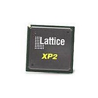
LFXP2-8E-5FTN256C Lattice, LFXP2-8E-5FTN256C Datasheet - Page 125

LFXP2-8E-5FTN256C
Manufacturer Part Number
LFXP2-8E-5FTN256C
Description
FPGA - Field Programmable Gate Array 8K LUTs 201I/O Inst- on DSP 1.2V -5 Spd
Manufacturer
Lattice
Datasheet
1.LFXP2-8E-5FTN256I.pdf
(341 pages)
Specifications of LFXP2-8E-5FTN256C
Number Of Macrocells
8000
Number Of Programmable I/os
201
Data Ram Size
226304
Supply Voltage (max)
1.26 V
Maximum Operating Temperature
+ 85 C
Minimum Operating Temperature
0 C
Mounting Style
SMD/SMT
Supply Voltage (min)
1.14 V
Package / Case
FTBGA-256
Lead Free Status / RoHS Status
Lead free / RoHS Compliant
Available stocks
Company
Part Number
Manufacturer
Quantity
Price
Company:
Part Number:
LFXP2-8E-5FTN256C
Manufacturer:
Lattice
Quantity:
63
Company:
Part Number:
LFXP2-8E-5FTN256C
Manufacturer:
Lattice Semiconductor Corporation
Quantity:
10 000
- Current page: 125 of 341
- Download datasheet (10Mb)
Lattice Semiconductor
Figure 9-2 describes the structure of the secondary clocks and edge clocks.
Figure 9-2. LatticeXP2 Secondary Clocks and Edge Clocks (LFXP2-40)
Primary Clock Note
The CLKOP must be used as the feedback source to optimize PLL performance.
Most designers use PLLs for clock tree injection removal mode and the CLKOP should be assigned to a primary
clock. This is done automatically by the software unless otherwise specified by the user.
CLKOP can route only to CLK0 to CLK5, while CLKOS/CLKOK can route to all primary clocks (CLK0 TO CLK7).
When CLK6 or CLK7 is used as a primary clock and there is only one clock input to the DCS, the DCS is assigned
as a buffer mode by the software. Please see the DCS section of this document for detailed information.
Specifying Clocks in the Design Tools
If desired, designers can specify the clock resources, primary, secondary or edge to be used to distribute a given
clock source. Figure 9-3 illustrates how this can be done in the Pre-map Preference editor. Alternatively, the prefer-
ence file can be used, as discussed in Appendix C.
Primary-Pure and Primary-DCS
Primary Clock Net can be assigned to either Primary-Pure (CLK0 to CLK5) or Primary-DCS (CLK6 and CLK7).
Global Primary Clock and Quadrant Primary Clock
Global Primary Clock
If a primary clock is not assigned as a quadrant clock, the software assumes it is a global clock.
There are six Global Primary/Pure clocks and two Global Primary/DCS clocks available.
ECLK1
ECLK1
Secondary Clock
Secondary Clock
Secondary Clock
Secondary Clock
sysIO Bank 0
sysIO Bank 5
Region 2
Region 3
Region 4
Region 1
DSP Row
DSP Row
EBR Row
9-3
Secondary Clock
Secondary Clock
Secondary Clock
Secondary Clock
Region 5
Region 6
Region 7
Region 8
sysIO Bank 1
sysIO Bank 4
ECLK2
ECLK2
LatticeXP2 sysCLOCK PLL
Design and Usage Guide
Related parts for LFXP2-8E-5FTN256C
Image
Part Number
Description
Manufacturer
Datasheet
Request
R

Part Number:
Description:
FPGA - Field Programmable Gate Array 8K LUTs 100I/O Inst- on DSP 1.2V -5 Spd
Manufacturer:
Lattice
Datasheet:

Part Number:
Description:
FPGA - Field Programmable Gate Array 8K LUTs 201 I/O Inst on DSP 1.2V -5 Spd
Manufacturer:
Lattice
Datasheet:

Part Number:
Description:
FPGA - Field Programmable Gate Array 8K LUTs 100 I/O Inst on DSP 1.2V -5 Spd
Manufacturer:
Lattice
Datasheet:

Part Number:
Description:
IC, LATTICEXP2 FPGA, 435MHZ, QFP-208
Manufacturer:
LATTICE SEMICONDUCTOR
Datasheet:

Part Number:
Description:
FPGA - Field Programmable Gate Array 8K LUTs 86I/O Inst- on DSP 1.2V -5 Spd
Manufacturer:
Lattice

Part Number:
Description:
FPGA - Field Programmable Gate Array 8K LUTs 201I/O Inst- on DSP 1.2V -7 Spd
Manufacturer:
Lattice
Datasheet:
Part Number:
Description:
FPGA LatticeXP2 Family 8000 Cells Flash Technology 1.2V 144-Pin TQFP
Manufacturer:
LATTICE SEMICONDUCTOR
Datasheet:

Part Number:
Description:
IC DSP 8KLUTS 146I/O 208PQFP
Manufacturer:
Lattice
Datasheet:

Part Number:
Description:
IC DSP 8KLUTS 100I/O 144TQFP
Manufacturer:
Lattice
Datasheet:

Part Number:
Description:
IC DSP 8KLUTS 86I/O 132CSBGA
Manufacturer:
Lattice
Datasheet:

Part Number:
Description:
IC DSP 8KLUTS 86I/O 132CSBGA
Manufacturer:
Lattice
Datasheet:

Part Number:
Description:
IC DSP 8KLUTS 146I/O 208PQFP
Manufacturer:
Lattice
Datasheet:

Part Number:
Description:
IC DSP 8KLUTS 201I/O 256FTBGA
Manufacturer:
Lattice
Datasheet:

Part Number:
Description:
IC FPGA 8KLUTS 86I/O 132-BGA
Manufacturer:
Lattice
Datasheet:

Part Number:
Description:
IC FPGA 8KLUTS 86I/O 132-BGA
Manufacturer:
Lattice
Datasheet:


