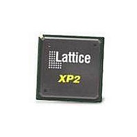
LFXP2-8E-5FTN256C Lattice, LFXP2-8E-5FTN256C Datasheet - Page 198

LFXP2-8E-5FTN256C
Manufacturer Part Number
LFXP2-8E-5FTN256C
Description
FPGA - Field Programmable Gate Array 8K LUTs 201I/O Inst- on DSP 1.2V -5 Spd
Manufacturer
Lattice
Datasheet
1.LFXP2-8E-5FTN256I.pdf
(341 pages)
Specifications of LFXP2-8E-5FTN256C
Number Of Macrocells
8000
Number Of Programmable I/os
201
Data Ram Size
226304
Supply Voltage (max)
1.26 V
Maximum Operating Temperature
+ 85 C
Minimum Operating Temperature
0 C
Mounting Style
SMD/SMT
Supply Voltage (min)
1.14 V
Package / Case
FTBGA-256
Lead Free Status / RoHS Status
Lead free / RoHS Compliant
Available stocks
Company
Part Number
Manufacturer
Quantity
Price
Company:
Part Number:
LFXP2-8E-5FTN256C
Manufacturer:
Lattice
Quantity:
63
Company:
Part Number:
LFXP2-8E-5FTN256C
Manufacturer:
Lattice Semiconductor Corporation
Quantity:
10 000
- Current page: 198 of 341
- Download datasheet (10Mb)
Lattice Semiconductor
Delay time = 20 x 1/frequency.
The transfer delay time, including the extra delay time to enable the Flash circuitry, is 5uS minimum. The clock fre-
quency can then be set to 2.5 MHz if continuous clocking is desired.
When all the data captured into the data buffer are shifted out, additional clocks will shift out dummy data. The SI
pin is not connected to the input of the data buffer when the READ_TAG command is shifted into the device. While
the data in the data buffer is shifted out to the direction of SO, dummy data is shifted into the data buffer. Conse-
quently, when over-shifting occurs, dummy data of unknown value is shifted out.
Figure 10-57. Readout Order
Figure 10-58. READ_TAG Waveform
STATUS (4Ah)
The STATUS command allows the single-bit status register to be read. This command can be loaded at any time
after the WRITE_EN command has already been shifted into the device first. This command does not terminate
the programming or erase action. It is used to report the progress of the programming or erase action.
The status register actual size is only 1 bit. Dummy data is shifted out on the SO pin if extra data shifting clocks are
applied. The command can be shifted into the device again to capture the status bit and then read out.
During the interval of shifting the command, the additional programming or erase time is provided by driving the
Chip Select pin to high and holding the CLK pin low. Clocking while holding the Chip Select pin high is optional.
If the maximum programming time or erasure has expired and the status bit still is not set to 1, then erase or pro-
gramming has failed.
CS
CLK
SI
SO
Cell N-1
Flash
8 Bits READ_TAG
Command
Bit N-1
Bit N-1
Time elapsed must be 5µs
24 Bits Dummy
Flash Memory Cells
HI-Z
If the clock is too fast
add delay before
Data capture
21st clock
21st clock
starts at
10-48
0 1 2
LatticeXP2 Memory Usage Guide
TAG Memory Data
Enable SO on 24th Dummy Clock.
Bit 0 is valid.
Bit 0
Bit 0
Cell 0
Flash
SO
N-1
HI-Z
Related parts for LFXP2-8E-5FTN256C
Image
Part Number
Description
Manufacturer
Datasheet
Request
R

Part Number:
Description:
FPGA - Field Programmable Gate Array 8K LUTs 100I/O Inst- on DSP 1.2V -5 Spd
Manufacturer:
Lattice
Datasheet:

Part Number:
Description:
FPGA - Field Programmable Gate Array 8K LUTs 201 I/O Inst on DSP 1.2V -5 Spd
Manufacturer:
Lattice
Datasheet:

Part Number:
Description:
FPGA - Field Programmable Gate Array 8K LUTs 100 I/O Inst on DSP 1.2V -5 Spd
Manufacturer:
Lattice
Datasheet:

Part Number:
Description:
IC, LATTICEXP2 FPGA, 435MHZ, QFP-208
Manufacturer:
LATTICE SEMICONDUCTOR
Datasheet:

Part Number:
Description:
FPGA - Field Programmable Gate Array 8K LUTs 86I/O Inst- on DSP 1.2V -5 Spd
Manufacturer:
Lattice

Part Number:
Description:
FPGA - Field Programmable Gate Array 8K LUTs 201I/O Inst- on DSP 1.2V -7 Spd
Manufacturer:
Lattice
Datasheet:
Part Number:
Description:
FPGA LatticeXP2 Family 8000 Cells Flash Technology 1.2V 144-Pin TQFP
Manufacturer:
LATTICE SEMICONDUCTOR
Datasheet:

Part Number:
Description:
IC DSP 8KLUTS 146I/O 208PQFP
Manufacturer:
Lattice
Datasheet:

Part Number:
Description:
IC DSP 8KLUTS 100I/O 144TQFP
Manufacturer:
Lattice
Datasheet:

Part Number:
Description:
IC DSP 8KLUTS 86I/O 132CSBGA
Manufacturer:
Lattice
Datasheet:

Part Number:
Description:
IC DSP 8KLUTS 86I/O 132CSBGA
Manufacturer:
Lattice
Datasheet:

Part Number:
Description:
IC DSP 8KLUTS 146I/O 208PQFP
Manufacturer:
Lattice
Datasheet:

Part Number:
Description:
IC DSP 8KLUTS 201I/O 256FTBGA
Manufacturer:
Lattice
Datasheet:

Part Number:
Description:
IC FPGA 8KLUTS 86I/O 132-BGA
Manufacturer:
Lattice
Datasheet:

Part Number:
Description:
IC FPGA 8KLUTS 86I/O 132-BGA
Manufacturer:
Lattice
Datasheet:


