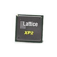
LFXP2-8E-5FTN256C Lattice, LFXP2-8E-5FTN256C Datasheet - Page 202

LFXP2-8E-5FTN256C
Manufacturer Part Number
LFXP2-8E-5FTN256C
Description
FPGA - Field Programmable Gate Array 8K LUTs 201I/O Inst- on DSP 1.2V -5 Spd
Manufacturer
Lattice
Datasheet
1.LFXP2-8E-5FTN256I.pdf
(341 pages)
Specifications of LFXP2-8E-5FTN256C
Number Of Macrocells
8000
Number Of Programmable I/os
201
Data Ram Size
226304
Supply Voltage (max)
1.26 V
Maximum Operating Temperature
+ 85 C
Minimum Operating Temperature
0 C
Mounting Style
SMD/SMT
Supply Voltage (min)
1.14 V
Package / Case
FTBGA-256
Lead Free Status / RoHS Status
Lead free / RoHS Compliant
Available stocks
Company
Part Number
Manufacturer
Quantity
Price
Company:
Part Number:
LFXP2-8E-5FTN256C
Manufacturer:
Lattice
Quantity:
63
Company:
Part Number:
LFXP2-8E-5FTN256C
Manufacturer:
Lattice Semiconductor Corporation
Quantity:
10 000
- Current page: 202 of 341
- Download datasheet (10Mb)
Lattice Semiconductor
Users need not specify data at all address locations. If data is not specified at certain address, the data at that loca-
tion is initialized to 0. IPexpress makes memory initialization possible both through the synthesis and simulation
flows.
FlashBak™ Capability
The LatticeXP2 FPGA family offers FlashBak capability, which is a way to store the data in the EBRs to the Flash
memory upon user command. This protects the user’s data from being lost when the system is powered off. The
FlashBak module (STFA primitive) has a single-command-two-operation process (see Figure 10-61). When the
FlashBak operation is initiated, an erase-UFM-Flash signal is enabled to erase the Flash, followed by the transfer-
to-flash operation. Once the transfer is done, the Flash controller sends a transfer-done signal back to the user
logic. During the FlashBak operation, the EBRs are not accessible. There is no difference between the regular EBR
RAM configuration and the shadow Flash (UFM) EBR RAM configuration in the ispLEVER GUI. The presence of
the STFA (FlashBak) primitive in a design determines the EBR RAM configuration. FlashBak cannot be used if the
soft-error detect (SED) is operating in an Always mode. Since there is no addressing but just a ‘dump’ of all EBR to
Flash, only one STFA module is necessary. Multiple modules are not necessary or allowed.
Figure 10-61. FlashBak Primitive
Figure 10-62. FlashBak Waveform
Table 10-22. STFA Port Descriptions
Technical Support Assistance
Hotline: 1-800-LATTICE (North America)
e-mail:
Internet: www.latticesemi.com
STOREN
UFMFAIL
UFMBUSYN
Port Name
+1-503-268-8001 (Outside North America)
techsupport@latticesemi.com
Hardware Port Name
Corresponding
storecmdn
fl_busyn
ufm_fail
UFM BUSYN
STOREN
STOREN
Minimum pulse width = 780ns
whether STOREN is released
I/O
1.85µs delay regardless of
O
O
I
Initiates to store the EBR content to Flash
Store to Flash operation failed
Tells the user whether the Flash is in the busy state or not
10-52
UFMBUSYN
UFMFAIL
STFA
LatticeXP2 Memory Usage Guide
Description
Related parts for LFXP2-8E-5FTN256C
Image
Part Number
Description
Manufacturer
Datasheet
Request
R

Part Number:
Description:
FPGA - Field Programmable Gate Array 8K LUTs 100I/O Inst- on DSP 1.2V -5 Spd
Manufacturer:
Lattice
Datasheet:

Part Number:
Description:
FPGA - Field Programmable Gate Array 8K LUTs 201 I/O Inst on DSP 1.2V -5 Spd
Manufacturer:
Lattice
Datasheet:

Part Number:
Description:
FPGA - Field Programmable Gate Array 8K LUTs 100 I/O Inst on DSP 1.2V -5 Spd
Manufacturer:
Lattice
Datasheet:

Part Number:
Description:
IC, LATTICEXP2 FPGA, 435MHZ, QFP-208
Manufacturer:
LATTICE SEMICONDUCTOR
Datasheet:

Part Number:
Description:
FPGA - Field Programmable Gate Array 8K LUTs 86I/O Inst- on DSP 1.2V -5 Spd
Manufacturer:
Lattice

Part Number:
Description:
FPGA - Field Programmable Gate Array 8K LUTs 201I/O Inst- on DSP 1.2V -7 Spd
Manufacturer:
Lattice
Datasheet:
Part Number:
Description:
FPGA LatticeXP2 Family 8000 Cells Flash Technology 1.2V 144-Pin TQFP
Manufacturer:
LATTICE SEMICONDUCTOR
Datasheet:

Part Number:
Description:
IC DSP 8KLUTS 146I/O 208PQFP
Manufacturer:
Lattice
Datasheet:

Part Number:
Description:
IC DSP 8KLUTS 100I/O 144TQFP
Manufacturer:
Lattice
Datasheet:

Part Number:
Description:
IC DSP 8KLUTS 86I/O 132CSBGA
Manufacturer:
Lattice
Datasheet:

Part Number:
Description:
IC DSP 8KLUTS 86I/O 132CSBGA
Manufacturer:
Lattice
Datasheet:

Part Number:
Description:
IC DSP 8KLUTS 146I/O 208PQFP
Manufacturer:
Lattice
Datasheet:

Part Number:
Description:
IC DSP 8KLUTS 201I/O 256FTBGA
Manufacturer:
Lattice
Datasheet:

Part Number:
Description:
IC FPGA 8KLUTS 86I/O 132-BGA
Manufacturer:
Lattice
Datasheet:

Part Number:
Description:
IC FPGA 8KLUTS 86I/O 132-BGA
Manufacturer:
Lattice
Datasheet:


