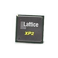
LFXP2-8E-5FTN256C Lattice, LFXP2-8E-5FTN256C Datasheet - Page 224

LFXP2-8E-5FTN256C
Manufacturer Part Number
LFXP2-8E-5FTN256C
Description
FPGA - Field Programmable Gate Array 8K LUTs 201I/O Inst- on DSP 1.2V -5 Spd
Manufacturer
Lattice
Datasheet
1.LFXP2-8E-5FTN256I.pdf
(341 pages)
Specifications of LFXP2-8E-5FTN256C
Number Of Macrocells
8000
Number Of Programmable I/os
201
Data Ram Size
226304
Supply Voltage (max)
1.26 V
Maximum Operating Temperature
+ 85 C
Minimum Operating Temperature
0 C
Mounting Style
SMD/SMT
Supply Voltage (min)
1.14 V
Package / Case
FTBGA-256
Lead Free Status / RoHS Status
Lead free / RoHS Compliant
Available stocks
Company
Part Number
Manufacturer
Quantity
Price
Company:
Part Number:
LFXP2-8E-5FTN256C
Manufacturer:
Lattice
Quantity:
63
Company:
Part Number:
LFXP2-8E-5FTN256C
Manufacturer:
Lattice Semiconductor Corporation
Quantity:
10 000
- Current page: 224 of 341
- Download datasheet (10Mb)
Lattice Semiconductor
All DDR output signals (“ADDR, CMD”, DQS, DQ, DM) are initially aligned to the rising edge of the FPGA clock
inside the FPGA core. The relative phase of the signals may be adjusted in the IOL logic before departing the
FPGA. These adjustments are shown in Figure 11-24.
LatticeXP2 devices contain DDR output and tri-state registers along with the DQSXFER signal generated by the
DQSBUFC that allows easy implementation of the write portion of the DDR memory interfaces. The DDR output
registers can be accessed in the design tools via the ODDRMXA and the ODDRXC primitives.
The DQS signal and the DDR clock outputs are generated using the ODDRXC primitive. As shown in the figure, the
CLKP and DQS signals are generated so that they are 180 degrees in phase with the clock. This is done by con-
necting “1” to the DA input and “0” to the DB inputs of the ODDRXC primitive. Refer to the DDR Generic Software
Primitive section of this document to see the ODDRXC timing waveforms.
The DDR clock output is then fed into a SSTL differential output buffer to generate CLKP and CLKN differential
clocks. Generating the CLKN in this manner prevents any skew between the two signals. When interfacing to
DDR1, SDRAM memory CLKP should be connected to the SSTL25D I/O standard. When interfacing to DDR2
memory, it should be connected to the SSTL18D I/O standard.
The DQSXFER output from the DQSBUFC block is the 90-degree phase shifted clock. This 90-degree phase
shifted clock is used as an input to the ODDRMXA block. The ODDRMXA is used to generate the DQ and DM data
outputs going to the memory. In the ODDRMXA module, the data is first registered using the ECLK or FPGA clock
input and then shifted out using the DQSXFER signal. To ensure that the data going to the memory is center-
aligned to the DQS, the DQSXFER is inverted inside the ODDRXMA primitive. This will generate data that is cen-
ter-aligned to the DQS. Refer to the Software Primitives section of this document for the ODDRXMA timing wave-
forms.
The DDR interface specification for t
times must be met. This is accomplished by ensuring that the CLKP and DQS signals are identical in phase.
The tristate control for the DQS and DQ outputs can also be implemented using the ODDRXC primitive.
Figure 11-24 shows the DDR Write implementation using the DDR primitives.
3. The controller must meet the DDR interface specification for t
4. The DDR output data must be muxed from two SDR streams into a single outgoing DDR data stream.
falling to CLKP rising setup and hold times.
DSS
and t
DSH
parameters defined as DQS falling to CLKP rising setup and hold
11-20
LatticeXP2 High-Speed I/O Interface
DSS
and t
DSH
parameters, defined as DQS
Related parts for LFXP2-8E-5FTN256C
Image
Part Number
Description
Manufacturer
Datasheet
Request
R

Part Number:
Description:
FPGA - Field Programmable Gate Array 8K LUTs 100I/O Inst- on DSP 1.2V -5 Spd
Manufacturer:
Lattice
Datasheet:

Part Number:
Description:
FPGA - Field Programmable Gate Array 8K LUTs 201 I/O Inst on DSP 1.2V -5 Spd
Manufacturer:
Lattice
Datasheet:

Part Number:
Description:
FPGA - Field Programmable Gate Array 8K LUTs 100 I/O Inst on DSP 1.2V -5 Spd
Manufacturer:
Lattice
Datasheet:

Part Number:
Description:
IC, LATTICEXP2 FPGA, 435MHZ, QFP-208
Manufacturer:
LATTICE SEMICONDUCTOR
Datasheet:

Part Number:
Description:
FPGA - Field Programmable Gate Array 8K LUTs 86I/O Inst- on DSP 1.2V -5 Spd
Manufacturer:
Lattice

Part Number:
Description:
FPGA - Field Programmable Gate Array 8K LUTs 201I/O Inst- on DSP 1.2V -7 Spd
Manufacturer:
Lattice
Datasheet:
Part Number:
Description:
FPGA LatticeXP2 Family 8000 Cells Flash Technology 1.2V 144-Pin TQFP
Manufacturer:
LATTICE SEMICONDUCTOR
Datasheet:

Part Number:
Description:
IC DSP 8KLUTS 146I/O 208PQFP
Manufacturer:
Lattice
Datasheet:

Part Number:
Description:
IC DSP 8KLUTS 100I/O 144TQFP
Manufacturer:
Lattice
Datasheet:

Part Number:
Description:
IC DSP 8KLUTS 86I/O 132CSBGA
Manufacturer:
Lattice
Datasheet:

Part Number:
Description:
IC DSP 8KLUTS 86I/O 132CSBGA
Manufacturer:
Lattice
Datasheet:

Part Number:
Description:
IC DSP 8KLUTS 146I/O 208PQFP
Manufacturer:
Lattice
Datasheet:

Part Number:
Description:
IC DSP 8KLUTS 201I/O 256FTBGA
Manufacturer:
Lattice
Datasheet:

Part Number:
Description:
IC FPGA 8KLUTS 86I/O 132-BGA
Manufacturer:
Lattice
Datasheet:

Part Number:
Description:
IC FPGA 8KLUTS 86I/O 132-BGA
Manufacturer:
Lattice
Datasheet:


