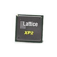
LFXP2-8E-5FTN256C Lattice, LFXP2-8E-5FTN256C Datasheet - Page 158

LFXP2-8E-5FTN256C
Manufacturer Part Number
LFXP2-8E-5FTN256C
Description
FPGA - Field Programmable Gate Array 8K LUTs 201I/O Inst- on DSP 1.2V -5 Spd
Manufacturer
Lattice
Datasheet
1.LFXP2-8E-5FTN256I.pdf
(341 pages)
Specifications of LFXP2-8E-5FTN256C
Number Of Macrocells
8000
Number Of Programmable I/os
201
Data Ram Size
226304
Supply Voltage (max)
1.26 V
Maximum Operating Temperature
+ 85 C
Minimum Operating Temperature
0 C
Mounting Style
SMD/SMT
Supply Voltage (min)
1.14 V
Package / Case
FTBGA-256
Lead Free Status / RoHS Status
Lead free / RoHS Compliant
Available stocks
Company
Part Number
Manufacturer
Quantity
Price
Company:
Part Number:
LFXP2-8E-5FTN256C
Manufacturer:
Lattice
Quantity:
63
Company:
Part Number:
LFXP2-8E-5FTN256C
Manufacturer:
Lattice Semiconductor Corporation
Quantity:
10 000
- Current page: 158 of 341
- Download datasheet (10Mb)
Lattice Semiconductor
Table 10-4. Single Port RAM Attributes for LatticeXP2
The Single Port RAM (RAM_DQ) can be configured as NORMAL or WRITE THROUGH modes. Each of these
modes affects the data coming out of port Q of the memory during the write operation followed by the read opera-
tion at the same memory location.
Additionally, users can select to enable the output registers for RAM_DQ. Figures 10-6-10-9 show the internal tim-
ing waveforms for the Single Port RAM (RAM_DQ) with these options.
Address depth
Data Width
Enable Output Registers
Enable GSR
Reset Mode
Memory File Format
Write Mode
Chip Select Decode
Init Value
Attribute
Address Depth Read Port
Data Word Width Read Port
Register Mode (Pipelining)
for Write Port
Enables Global Set Reset
Read / Write Mode for Write
Port
Chip Select Decode for
Read Port
Initialization value
Selects the Reset type
Description
16K, 8K, 4K, 2K, 1K, 512
1, 2, 4, 9, 18, 36
NOREG, OUTREG
ENABLE, DISABLE
ASYNC, SYNC
BINARY, HEX, ADDRESSED
HEX
NORMAL, WRITE-
THROUGH
0b000, 0b001, 0b010,
0b011, 0b100, 0b101,
0b110, 0b111
0x000000000000000000000
00000000000000000000000
00000000000000000000000
0000000000000......0xFFFF
FFFFFFFFFFFFFFFFFFFFF
FFFFFFFFFFFFFFFFFFFFF
FFFFFFFFFFFFFFFFFFFFF
FFFFFFFFFFFFF
10-8
Values
LatticeXP2 Memory Usage Guide
1
NOREG
ENABLE
ASYNC
NORMAL
0b000
0x000000000
00000000000
00000000000
00000000000
00000000000
00000000000
00000000000
00000
Default Value
Through IPexpress
User Selectable
YES
YES
YES
YES
YES
YES
YES
NO
NO
Related parts for LFXP2-8E-5FTN256C
Image
Part Number
Description
Manufacturer
Datasheet
Request
R

Part Number:
Description:
FPGA - Field Programmable Gate Array 8K LUTs 100I/O Inst- on DSP 1.2V -5 Spd
Manufacturer:
Lattice
Datasheet:

Part Number:
Description:
FPGA - Field Programmable Gate Array 8K LUTs 201 I/O Inst on DSP 1.2V -5 Spd
Manufacturer:
Lattice
Datasheet:

Part Number:
Description:
FPGA - Field Programmable Gate Array 8K LUTs 100 I/O Inst on DSP 1.2V -5 Spd
Manufacturer:
Lattice
Datasheet:

Part Number:
Description:
IC, LATTICEXP2 FPGA, 435MHZ, QFP-208
Manufacturer:
LATTICE SEMICONDUCTOR
Datasheet:

Part Number:
Description:
FPGA - Field Programmable Gate Array 8K LUTs 86I/O Inst- on DSP 1.2V -5 Spd
Manufacturer:
Lattice

Part Number:
Description:
FPGA - Field Programmable Gate Array 8K LUTs 201I/O Inst- on DSP 1.2V -7 Spd
Manufacturer:
Lattice
Datasheet:
Part Number:
Description:
FPGA LatticeXP2 Family 8000 Cells Flash Technology 1.2V 144-Pin TQFP
Manufacturer:
LATTICE SEMICONDUCTOR
Datasheet:

Part Number:
Description:
IC DSP 8KLUTS 146I/O 208PQFP
Manufacturer:
Lattice
Datasheet:

Part Number:
Description:
IC DSP 8KLUTS 100I/O 144TQFP
Manufacturer:
Lattice
Datasheet:

Part Number:
Description:
IC DSP 8KLUTS 86I/O 132CSBGA
Manufacturer:
Lattice
Datasheet:

Part Number:
Description:
IC DSP 8KLUTS 86I/O 132CSBGA
Manufacturer:
Lattice
Datasheet:

Part Number:
Description:
IC DSP 8KLUTS 146I/O 208PQFP
Manufacturer:
Lattice
Datasheet:

Part Number:
Description:
IC DSP 8KLUTS 201I/O 256FTBGA
Manufacturer:
Lattice
Datasheet:

Part Number:
Description:
IC FPGA 8KLUTS 86I/O 132-BGA
Manufacturer:
Lattice
Datasheet:

Part Number:
Description:
IC FPGA 8KLUTS 86I/O 132-BGA
Manufacturer:
Lattice
Datasheet:


