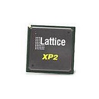
LFXP2-8E-5FTN256C Lattice, LFXP2-8E-5FTN256C Datasheet - Page 200

LFXP2-8E-5FTN256C
Manufacturer Part Number
LFXP2-8E-5FTN256C
Description
FPGA - Field Programmable Gate Array 8K LUTs 201I/O Inst- on DSP 1.2V -5 Spd
Manufacturer
Lattice
Datasheet
1.LFXP2-8E-5FTN256I.pdf
(341 pages)
Specifications of LFXP2-8E-5FTN256C
Number Of Macrocells
8000
Number Of Programmable I/os
201
Data Ram Size
226304
Supply Voltage (max)
1.26 V
Maximum Operating Temperature
+ 85 C
Minimum Operating Temperature
0 C
Mounting Style
SMD/SMT
Supply Voltage (min)
1.14 V
Package / Case
FTBGA-256
Lead Free Status / RoHS Status
Lead free / RoHS Compliant
Available stocks
Company
Part Number
Manufacturer
Quantity
Price
Company:
Part Number:
LFXP2-8E-5FTN256C
Manufacturer:
Lattice
Quantity:
63
Company:
Part Number:
LFXP2-8E-5FTN256C
Manufacturer:
Lattice Semiconductor Corporation
Quantity:
10 000
- Current page: 200 of 341
- Download datasheet (10Mb)
Lattice Semiconductor
LatticeXP2 Memory Usage Guide
Availability of TAG Memory
TAG memory is available most of time on the Slave SPI interface with the following exceptions:
• When the SRAM fuses are being accessed by the JTAG port, Slave SPI interface or refreshing
• When the other Flash cells are being accessed through the JTAG port or Slave SPI interface
• While JTAG BSCAN testing is taking place
• The Slave SPI interface is disabled with the persistent fuse programmed (set to off)
AC Timing
• 25 MHz maximum CLK
• 5 uS minimum read command delay
• 2 mS minimum delay from VCCmin to shifting in the first command
Programming Timing
• 1 sec. maximum erase time
• 5 mS maximum programming time
Programming via the JTAG Interface
.VME files can be generated for the ispVM System software which only programs the TAG memory. These .VME
files are handled according to the standard ispVME flow.
Initializing Memory
In the EBR based ROM or RAM memory modes and the PFU based ROM memory mode, it is possible to specify
the power-on state of each bit in the memory array. Each bit in the memory array can have one of two values: 0 or
1.
Initialization File Format
The initialization file is an ASCII file, which users can create or edit using any ASCII editor. IPexpress supports
three types of memory file formats:
• Binary file
• Hex File
• Addressed Hex
The file name for the memory initialization file is *.mem (<file_name>.mem). Each row depicts the value to be
stored in a particular memory location and the number of characters (or the number of columns) represents the
number of bits for each address (or the width of the memory module).
The Initialization File is primarily used for configuring the ROMs. The EBR in RAM mode can optionally use this Ini-
tialization File also to preload the memory contents.
The TAG memory uses hex or binary non-addressed files. Since it is a SPI, it cannot use the addressed hex file.
10-50
Related parts for LFXP2-8E-5FTN256C
Image
Part Number
Description
Manufacturer
Datasheet
Request
R

Part Number:
Description:
FPGA - Field Programmable Gate Array 8K LUTs 100I/O Inst- on DSP 1.2V -5 Spd
Manufacturer:
Lattice
Datasheet:

Part Number:
Description:
FPGA - Field Programmable Gate Array 8K LUTs 201 I/O Inst on DSP 1.2V -5 Spd
Manufacturer:
Lattice
Datasheet:

Part Number:
Description:
FPGA - Field Programmable Gate Array 8K LUTs 100 I/O Inst on DSP 1.2V -5 Spd
Manufacturer:
Lattice
Datasheet:

Part Number:
Description:
IC, LATTICEXP2 FPGA, 435MHZ, QFP-208
Manufacturer:
LATTICE SEMICONDUCTOR
Datasheet:

Part Number:
Description:
FPGA - Field Programmable Gate Array 8K LUTs 86I/O Inst- on DSP 1.2V -5 Spd
Manufacturer:
Lattice

Part Number:
Description:
FPGA - Field Programmable Gate Array 8K LUTs 201I/O Inst- on DSP 1.2V -7 Spd
Manufacturer:
Lattice
Datasheet:
Part Number:
Description:
FPGA LatticeXP2 Family 8000 Cells Flash Technology 1.2V 144-Pin TQFP
Manufacturer:
LATTICE SEMICONDUCTOR
Datasheet:

Part Number:
Description:
IC DSP 8KLUTS 146I/O 208PQFP
Manufacturer:
Lattice
Datasheet:

Part Number:
Description:
IC DSP 8KLUTS 100I/O 144TQFP
Manufacturer:
Lattice
Datasheet:

Part Number:
Description:
IC DSP 8KLUTS 86I/O 132CSBGA
Manufacturer:
Lattice
Datasheet:

Part Number:
Description:
IC DSP 8KLUTS 86I/O 132CSBGA
Manufacturer:
Lattice
Datasheet:

Part Number:
Description:
IC DSP 8KLUTS 146I/O 208PQFP
Manufacturer:
Lattice
Datasheet:

Part Number:
Description:
IC DSP 8KLUTS 201I/O 256FTBGA
Manufacturer:
Lattice
Datasheet:

Part Number:
Description:
IC FPGA 8KLUTS 86I/O 132-BGA
Manufacturer:
Lattice
Datasheet:

Part Number:
Description:
IC FPGA 8KLUTS 86I/O 132-BGA
Manufacturer:
Lattice
Datasheet:


