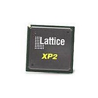
LFXP2-8E-5FTN256C Lattice, LFXP2-8E-5FTN256C Datasheet - Page 16

LFXP2-8E-5FTN256C
Manufacturer Part Number
LFXP2-8E-5FTN256C
Description
FPGA - Field Programmable Gate Array 8K LUTs 201I/O Inst- on DSP 1.2V -5 Spd
Manufacturer
Lattice
Datasheet
1.LFXP2-8E-5FTN256I.pdf
(341 pages)
Specifications of LFXP2-8E-5FTN256C
Number Of Macrocells
8000
Number Of Programmable I/os
201
Data Ram Size
226304
Supply Voltage (max)
1.26 V
Maximum Operating Temperature
+ 85 C
Minimum Operating Temperature
0 C
Mounting Style
SMD/SMT
Supply Voltage (min)
1.14 V
Package / Case
FTBGA-256
Lead Free Status / RoHS Status
Lead free / RoHS Compliant
Available stocks
Company
Part Number
Manufacturer
Quantity
Price
Company:
Part Number:
LFXP2-8E-5FTN256C
Manufacturer:
Lattice
Quantity:
63
Company:
Part Number:
LFXP2-8E-5FTN256C
Manufacturer:
Lattice Semiconductor Corporation
Quantity:
10 000
- Current page: 16 of 341
- Download datasheet (10Mb)
Lattice Semiconductor
Figure 2-1. Simplified Block Diagram, LatticeXP2-17 Device (Top Level)
PFU Blocks
The core of the LatticeXP2 device is made up of logic blocks in two forms, PFUs and PFFs. PFUs can be pro-
grammed to perform logic, arithmetic, distributed RAM and distributed ROM functions. PFF blocks can be pro-
grammed to perform logic, arithmetic and ROM functions. Except where necessary, the remainder of this data
sheet will use the term PFU to refer to both PFU and PFF blocks.
Each PFU block consists of four interconnected slices, numbered Slice 0 through Slice 3, as shown in Figure 2-2.
All the interconnections to and from PFU blocks are from routing. There are 50 inputs and 23 outputs associated
with each PFU block.
Programmable
Function Units
(PFUs)
sysMEM Block
RAM
DSP Blocks
SPI Port
On-chip
Oscillator
sysCLOCK PLLs
2-2
Flexible Routing
sysIO Buffers,
Pre-Engineered Source
Synchronous Support
LatticeXP2 Family Data Sheet
Architecture
JTAG Port
Flash
Related parts for LFXP2-8E-5FTN256C
Image
Part Number
Description
Manufacturer
Datasheet
Request
R

Part Number:
Description:
FPGA - Field Programmable Gate Array 8K LUTs 100I/O Inst- on DSP 1.2V -5 Spd
Manufacturer:
Lattice
Datasheet:

Part Number:
Description:
FPGA - Field Programmable Gate Array 8K LUTs 201 I/O Inst on DSP 1.2V -5 Spd
Manufacturer:
Lattice
Datasheet:

Part Number:
Description:
FPGA - Field Programmable Gate Array 8K LUTs 100 I/O Inst on DSP 1.2V -5 Spd
Manufacturer:
Lattice
Datasheet:

Part Number:
Description:
IC, LATTICEXP2 FPGA, 435MHZ, QFP-208
Manufacturer:
LATTICE SEMICONDUCTOR
Datasheet:

Part Number:
Description:
FPGA - Field Programmable Gate Array 8K LUTs 86I/O Inst- on DSP 1.2V -5 Spd
Manufacturer:
Lattice

Part Number:
Description:
FPGA - Field Programmable Gate Array 8K LUTs 201I/O Inst- on DSP 1.2V -7 Spd
Manufacturer:
Lattice
Datasheet:
Part Number:
Description:
FPGA LatticeXP2 Family 8000 Cells Flash Technology 1.2V 144-Pin TQFP
Manufacturer:
LATTICE SEMICONDUCTOR
Datasheet:

Part Number:
Description:
IC DSP 8KLUTS 146I/O 208PQFP
Manufacturer:
Lattice
Datasheet:

Part Number:
Description:
IC DSP 8KLUTS 100I/O 144TQFP
Manufacturer:
Lattice
Datasheet:

Part Number:
Description:
IC DSP 8KLUTS 86I/O 132CSBGA
Manufacturer:
Lattice
Datasheet:

Part Number:
Description:
IC DSP 8KLUTS 86I/O 132CSBGA
Manufacturer:
Lattice
Datasheet:

Part Number:
Description:
IC DSP 8KLUTS 146I/O 208PQFP
Manufacturer:
Lattice
Datasheet:

Part Number:
Description:
IC DSP 8KLUTS 201I/O 256FTBGA
Manufacturer:
Lattice
Datasheet:

Part Number:
Description:
IC FPGA 8KLUTS 86I/O 132-BGA
Manufacturer:
Lattice
Datasheet:

Part Number:
Description:
IC FPGA 8KLUTS 86I/O 132-BGA
Manufacturer:
Lattice
Datasheet:


