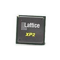
LFXP2-8E-5FTN256C Lattice, LFXP2-8E-5FTN256C Datasheet - Page 223

LFXP2-8E-5FTN256C
Manufacturer Part Number
LFXP2-8E-5FTN256C
Description
FPGA - Field Programmable Gate Array 8K LUTs 201I/O Inst- on DSP 1.2V -5 Spd
Manufacturer
Lattice
Datasheet
1.LFXP2-8E-5FTN256I.pdf
(341 pages)
Specifications of LFXP2-8E-5FTN256C
Number Of Macrocells
8000
Number Of Programmable I/os
201
Data Ram Size
226304
Supply Voltage (max)
1.26 V
Maximum Operating Temperature
+ 85 C
Minimum Operating Temperature
0 C
Mounting Style
SMD/SMT
Supply Voltage (min)
1.14 V
Package / Case
FTBGA-256
Lead Free Status / RoHS Status
Lead free / RoHS Compliant
Available stocks
Company
Part Number
Manufacturer
Quantity
Price
Company:
Part Number:
LFXP2-8E-5FTN256C
Manufacturer:
Lattice
Quantity:
63
Company:
Part Number:
LFXP2-8E-5FTN256C
Manufacturer:
Lattice Semiconductor Corporation
Quantity:
10 000
- Current page: 223 of 341
- Download datasheet (10Mb)
Lattice Semiconductor
Data Read Critical Path
Data in the second stage DDR registers can be registered either on the positive edge or on the falling edge of
FPGA clock depending on the DDRCLKPOL signal. In order to ensure that the data transferred to the FPGA core
registers is aligned to the rising edge of the system clock, this path should be constrained with a half clock transfer.
This half clock transfer can be forced in the software by assigning a multi-cycle constraint (multi-cycle of 0.5 X) on
all the data paths to first PFU register.
DQS Postamble
At the end of a READ cycle, the DDR SDRAM device executes the READ cycle postamble and then immediately
tristates both the DQ and DQS output drivers. Since neither the memory controller (FPGA) nor the DDR SDRAM
device are driving DQ or DQS at that time, these signals float to a level determined by the off-chip termination
resistors. While these signals are floating, noise on the DQS strobe may be interpreted as a valid strobe signal by
the FPGA input buffer. This can cause the last READ data captured in the IOL input DDR registers to be overwrit-
ten before the data has been transferred to the free running resynchronization registers inside the FPGA.
Figure 11-23. Postamble Effect on READ
LatticeXP2 devices have extra dedicated logic in the in the DQS Delay Block that prevents this postamble problem.
The DQS postamble logic is automatically implemented when the user instantiates the DQS Delay logic (DQS-
BUFC software primitive) in the design.
Memory Write Implementation
To implement the write portion of a DDR memory interface, two streams of single data rate data must be multi-
plexed together with data transitioning on both edges of the clock. In addition, during a write cycle, DQS must arrive
at the memory pins center-aligned with the data, DQ. Along with the DQS strobe and data this portion of the inter-
face must also provide the CLKP, CLKN Address/Command and Data Mask (DM) signals to the memory.
It is the responsibility of the FPGA output control to edge-align the DDR output signals (ADDR,CMD, DQS, but not
DQ, DM) to the rising edge of the outgoing differential clock (CLKP/CLKN).
Challenges encountered by the during Memory WRITE:
1. DQS needs to be center-aligned with the outgoing DDR Data, DQ.
2. Differential CLK signals (CLKP and CLKN) need to be generated.
DQS at PIN
DQS at IOL
DATAIN_N
DATAIN_P
DQ at PIN
DQ at IOL
synce reg
CLK at
C
A
B
P0
P0
11-19
P0
N0
N0
P1
P1
LatticeXP2 High-Speed I/O Interface
N0
P0
P0
N0
P1
N1
N1
N1
P1
Related parts for LFXP2-8E-5FTN256C
Image
Part Number
Description
Manufacturer
Datasheet
Request
R

Part Number:
Description:
FPGA - Field Programmable Gate Array 8K LUTs 100I/O Inst- on DSP 1.2V -5 Spd
Manufacturer:
Lattice
Datasheet:

Part Number:
Description:
FPGA - Field Programmable Gate Array 8K LUTs 201 I/O Inst on DSP 1.2V -5 Spd
Manufacturer:
Lattice
Datasheet:

Part Number:
Description:
FPGA - Field Programmable Gate Array 8K LUTs 100 I/O Inst on DSP 1.2V -5 Spd
Manufacturer:
Lattice
Datasheet:

Part Number:
Description:
IC, LATTICEXP2 FPGA, 435MHZ, QFP-208
Manufacturer:
LATTICE SEMICONDUCTOR
Datasheet:

Part Number:
Description:
FPGA - Field Programmable Gate Array 8K LUTs 86I/O Inst- on DSP 1.2V -5 Spd
Manufacturer:
Lattice

Part Number:
Description:
FPGA - Field Programmable Gate Array 8K LUTs 201I/O Inst- on DSP 1.2V -7 Spd
Manufacturer:
Lattice
Datasheet:
Part Number:
Description:
FPGA LatticeXP2 Family 8000 Cells Flash Technology 1.2V 144-Pin TQFP
Manufacturer:
LATTICE SEMICONDUCTOR
Datasheet:

Part Number:
Description:
IC DSP 8KLUTS 146I/O 208PQFP
Manufacturer:
Lattice
Datasheet:

Part Number:
Description:
IC DSP 8KLUTS 100I/O 144TQFP
Manufacturer:
Lattice
Datasheet:

Part Number:
Description:
IC DSP 8KLUTS 86I/O 132CSBGA
Manufacturer:
Lattice
Datasheet:

Part Number:
Description:
IC DSP 8KLUTS 86I/O 132CSBGA
Manufacturer:
Lattice
Datasheet:

Part Number:
Description:
IC DSP 8KLUTS 146I/O 208PQFP
Manufacturer:
Lattice
Datasheet:

Part Number:
Description:
IC DSP 8KLUTS 201I/O 256FTBGA
Manufacturer:
Lattice
Datasheet:

Part Number:
Description:
IC FPGA 8KLUTS 86I/O 132-BGA
Manufacturer:
Lattice
Datasheet:

Part Number:
Description:
IC FPGA 8KLUTS 86I/O 132-BGA
Manufacturer:
Lattice
Datasheet:


