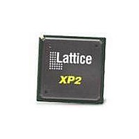
LFXP2-8E-5FTN256C Lattice, LFXP2-8E-5FTN256C Datasheet - Page 144

LFXP2-8E-5FTN256C
Manufacturer Part Number
LFXP2-8E-5FTN256C
Description
FPGA - Field Programmable Gate Array 8K LUTs 201I/O Inst- on DSP 1.2V -5 Spd
Manufacturer
Lattice
Datasheet
1.LFXP2-8E-5FTN256I.pdf
(341 pages)
Specifications of LFXP2-8E-5FTN256C
Number Of Macrocells
8000
Number Of Programmable I/os
201
Data Ram Size
226304
Supply Voltage (max)
1.26 V
Maximum Operating Temperature
+ 85 C
Minimum Operating Temperature
0 C
Mounting Style
SMD/SMT
Supply Voltage (min)
1.14 V
Package / Case
FTBGA-256
Lead Free Status / RoHS Status
Lead free / RoHS Compliant
Available stocks
Company
Part Number
Manufacturer
Quantity
Price
Company:
Part Number:
LFXP2-8E-5FTN256C
Manufacturer:
Lattice
Quantity:
63
Company:
Part Number:
LFXP2-8E-5FTN256C
Manufacturer:
Lattice Semiconductor Corporation
Quantity:
10 000
- Current page: 144 of 341
- Download datasheet (10Mb)
Lattice Semiconductor
)
-- synthesis translate_on
DCS Usage with Verilog - Example
module dcs(clk0,clk1,sel,dcsout);
input clk0, clk1, sel;
output dcsout;
DCS DCSInst0 (.SEL(sel),.CLK0(clk0),.CLK1(clk1),.DCSOUT(dcsout));
defparam DCSInst0.DCSMODE = “CLK0”;
endmodule
Oscillator (OSCE)
There is a dedicated oscillator in the LatticeXP2 device whose output is made available for users.
The oscillator frequency output is routed through a divider which is used as an input clock to the clock tree. The
available outputs of the divider are shown in Table 9-13. The oscillator frequency output can be further divided by
internal logic (user logic) for lower frequencies, if desired. The oscillator is powered down when not in use.
The output of this oscillator is not a precision clock. It is intended as an extra clock that does not require accurate
clocking.
Primitive Name: OSCE
Table 9-12. OSCE Port Definition
Table 9-13. OSCE Attribute Definition
OSC Primitive Symbol (OSCE)
Figure 9-21. OSC Symbol
Nominal Frequency
DCSMODE
PORT MAP (
User Attribute
=> “POS”
SEL
CLK0
CLK1
DCSOUT
);
Attribute Name
Output
NOM_FREQ
I/O
=>
=>
=>
=>
Name
clksel,
dcsclk0,
sysclk1,
dcsclk
OSC
OSCE
2.5, 3.14, 4.3, 5.4, 6.9, 8.1, 9.2, 10, 13, 15,
9-22
20, 26, 32, 40, 54, 80, 163
Oscillator Clock Output
OSC
Description
Value (MHz)
LatticeXP2 sysCLOCK PLL
Design and Usage Guide
Default Value
2.5
Related parts for LFXP2-8E-5FTN256C
Image
Part Number
Description
Manufacturer
Datasheet
Request
R

Part Number:
Description:
FPGA - Field Programmable Gate Array 8K LUTs 100I/O Inst- on DSP 1.2V -5 Spd
Manufacturer:
Lattice
Datasheet:

Part Number:
Description:
FPGA - Field Programmable Gate Array 8K LUTs 201 I/O Inst on DSP 1.2V -5 Spd
Manufacturer:
Lattice
Datasheet:

Part Number:
Description:
FPGA - Field Programmable Gate Array 8K LUTs 100 I/O Inst on DSP 1.2V -5 Spd
Manufacturer:
Lattice
Datasheet:

Part Number:
Description:
IC, LATTICEXP2 FPGA, 435MHZ, QFP-208
Manufacturer:
LATTICE SEMICONDUCTOR
Datasheet:

Part Number:
Description:
FPGA - Field Programmable Gate Array 8K LUTs 86I/O Inst- on DSP 1.2V -5 Spd
Manufacturer:
Lattice

Part Number:
Description:
FPGA - Field Programmable Gate Array 8K LUTs 201I/O Inst- on DSP 1.2V -7 Spd
Manufacturer:
Lattice
Datasheet:
Part Number:
Description:
FPGA LatticeXP2 Family 8000 Cells Flash Technology 1.2V 144-Pin TQFP
Manufacturer:
LATTICE SEMICONDUCTOR
Datasheet:

Part Number:
Description:
IC DSP 8KLUTS 146I/O 208PQFP
Manufacturer:
Lattice
Datasheet:

Part Number:
Description:
IC DSP 8KLUTS 100I/O 144TQFP
Manufacturer:
Lattice
Datasheet:

Part Number:
Description:
IC DSP 8KLUTS 86I/O 132CSBGA
Manufacturer:
Lattice
Datasheet:

Part Number:
Description:
IC DSP 8KLUTS 86I/O 132CSBGA
Manufacturer:
Lattice
Datasheet:

Part Number:
Description:
IC DSP 8KLUTS 146I/O 208PQFP
Manufacturer:
Lattice
Datasheet:

Part Number:
Description:
IC DSP 8KLUTS 201I/O 256FTBGA
Manufacturer:
Lattice
Datasheet:

Part Number:
Description:
IC FPGA 8KLUTS 86I/O 132-BGA
Manufacturer:
Lattice
Datasheet:

Part Number:
Description:
IC FPGA 8KLUTS 86I/O 132-BGA
Manufacturer:
Lattice
Datasheet:


