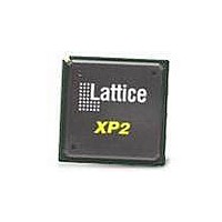
LFXP2-8E-5FTN256C Lattice, LFXP2-8E-5FTN256C Datasheet - Page 252

LFXP2-8E-5FTN256C
Manufacturer Part Number
LFXP2-8E-5FTN256C
Description
FPGA - Field Programmable Gate Array 8K LUTs 201I/O Inst- on DSP 1.2V -5 Spd
Manufacturer
Lattice
Datasheet
1.LFXP2-8E-5FTN256I.pdf
(341 pages)
Specifications of LFXP2-8E-5FTN256C
Number Of Macrocells
8000
Number Of Programmable I/os
201
Data Ram Size
226304
Supply Voltage (max)
1.26 V
Maximum Operating Temperature
+ 85 C
Minimum Operating Temperature
0 C
Mounting Style
SMD/SMT
Supply Voltage (min)
1.14 V
Package / Case
FTBGA-256
Lead Free Status / RoHS Status
Lead free / RoHS Compliant
Available stocks
Company
Part Number
Manufacturer
Quantity
Price
Company:
Part Number:
LFXP2-8E-5FTN256C
Manufacturer:
Lattice
Quantity:
63
Company:
Part Number:
LFXP2-8E-5FTN256C
Manufacturer:
Lattice Semiconductor Corporation
Quantity:
10 000
- Current page: 252 of 341
- Download datasheet (10Mb)
Lattice Semiconductor
Figure 12-7. Power Calculator Wizard Mode Window - Device Selection
In the following screens (Figures 8-12) users can select additional resources, such as I/O types, clock name, fre-
quency at which the clock in running and other parameters by selecting the appropriate resource using the pull-
down Type menu.
The number in these windows refers to the number of clocks and the index corresponds to each of the clocks. By
default, the clock names are clk_1, clk_2, and so on. Clock names can be changed by typing in the Clock Name
text box. For each clock domain and resource, parameters such as Frequency and Activity Factor can be specified.
In the final window, click the Create button for each clock driven resource to include the parameters specified for it.
1. Routing Resources
2. Logic
3. EBR
4. I/O
5. PLL
6. Clock Tree
12-8
Power Estimation and Management
for LatticeXP2 Devices
Related parts for LFXP2-8E-5FTN256C
Image
Part Number
Description
Manufacturer
Datasheet
Request
R

Part Number:
Description:
FPGA - Field Programmable Gate Array 8K LUTs 100I/O Inst- on DSP 1.2V -5 Spd
Manufacturer:
Lattice
Datasheet:

Part Number:
Description:
FPGA - Field Programmable Gate Array 8K LUTs 201 I/O Inst on DSP 1.2V -5 Spd
Manufacturer:
Lattice
Datasheet:

Part Number:
Description:
FPGA - Field Programmable Gate Array 8K LUTs 100 I/O Inst on DSP 1.2V -5 Spd
Manufacturer:
Lattice
Datasheet:

Part Number:
Description:
IC, LATTICEXP2 FPGA, 435MHZ, QFP-208
Manufacturer:
LATTICE SEMICONDUCTOR
Datasheet:

Part Number:
Description:
FPGA - Field Programmable Gate Array 8K LUTs 86I/O Inst- on DSP 1.2V -5 Spd
Manufacturer:
Lattice

Part Number:
Description:
FPGA - Field Programmable Gate Array 8K LUTs 201I/O Inst- on DSP 1.2V -7 Spd
Manufacturer:
Lattice
Datasheet:
Part Number:
Description:
FPGA LatticeXP2 Family 8000 Cells Flash Technology 1.2V 144-Pin TQFP
Manufacturer:
LATTICE SEMICONDUCTOR
Datasheet:

Part Number:
Description:
IC DSP 8KLUTS 146I/O 208PQFP
Manufacturer:
Lattice
Datasheet:

Part Number:
Description:
IC DSP 8KLUTS 100I/O 144TQFP
Manufacturer:
Lattice
Datasheet:

Part Number:
Description:
IC DSP 8KLUTS 86I/O 132CSBGA
Manufacturer:
Lattice
Datasheet:

Part Number:
Description:
IC DSP 8KLUTS 86I/O 132CSBGA
Manufacturer:
Lattice
Datasheet:

Part Number:
Description:
IC DSP 8KLUTS 146I/O 208PQFP
Manufacturer:
Lattice
Datasheet:

Part Number:
Description:
IC DSP 8KLUTS 201I/O 256FTBGA
Manufacturer:
Lattice
Datasheet:

Part Number:
Description:
IC FPGA 8KLUTS 86I/O 132-BGA
Manufacturer:
Lattice
Datasheet:

Part Number:
Description:
IC FPGA 8KLUTS 86I/O 132-BGA
Manufacturer:
Lattice
Datasheet:


