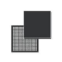
SPEAR300-2 STMicroelectronics, SPEAR300-2 Datasheet - Page 29

SPEAR300-2
Manufacturer Part Number
SPEAR300-2
Description
IC MPU ARM9 289LFBGA
Manufacturer
STMicroelectronics
Series
SPEAr®r
Datasheet
1.SPEAR300-2.pdf
(83 pages)
Specifications of SPEAR300-2
Processor Type
ARM Microprocessor
Speed
333MHz
Voltage
1.14 V ~ 3.6 V
Mounting Type
Surface Mount
Package / Case
289-LFBGA
Processor Series
SPEAr300
Core
ARM926EJ-S
Data Bus Width
16 bit
Maximum Clock Frequency
333 MHz
Operating Supply Voltage
1.2 V
Maximum Operating Temperature
+ 85 C
Mounting Style
SMD/SMT
Data Ram Size
56 KB
Interface Type
I2C, UART, USB, Serial
Number Of Programmable I/os
62
Number Of Timers
6
Program Memory Size
32 KB
Program Memory Type
ROM
Lead Free Status / RoHS Status
Lead free / RoHS Compliant
Features
-
Lead Free Status / Rohs Status
Lead free / RoHS Compliant
Other names
497-10849-5
Available stocks
Company
Part Number
Manufacturer
Quantity
Price
Company:
Part Number:
SPEAR300-2
Manufacturer:
ST
Quantity:
12 005
Part Number:
SPEAR300-2
Manufacturer:
ST
Quantity:
20 000
SPEAr300
3
3.1
3.2
Pin description
The following tables describe the pinout of the SPEAr300 listed by functional block.
List of abbreviations:
PU = Pull Up
PD = Pull Down
Required external components
1.
2.
3.
Dedicated pins
Table 2.
Table 3.
Master Clock
3.3 V Comp.
Group
GROUND
GROUND
Reset
ANALOG
DDR_COMP_1V8: place an external 121 kresistor between ball P4 and ball R4
USB_TX_RTUNE: connect an external 43.2 k pull-down resistor to ball K5
DIGITAL_REXT: place an external 121 k resistor between ball G4 and ball F4.
RTC
DIGITAL
Group
I/O
Power supply pin description
Master clock, RTC, Reset and 3.3 V comparator pin descriptions
DIGITAL_GND_R
DIGITAL_REXT
Signal name
MCLK_XO
MRESET#
MCLK_XI
RTC_XO
RTC_XI
Signal name
EX
AGND
VDD3
GND
Doc ID 16324 Rev 2
M17
Ball
G6, G7, G8, G9, G10, G11, H6, H7, H8, H9, H10,
H11, J6, J7, J8, J9, J10, J11, K6, K7, K8, K9, K10,
K11, L6, L7, L8, L9, L10, M8, M9, M10
F2, G1, J2, L1, L3, L5, N2, N4, P3, R3,N12
F5, F6, F7, F10, F11, F12, G5, J12, K12, L12, M12
G4
P1
P2
E2
E1
F4
Direction
Output
Output
Output
Power
Input
Input
Input
32 kHz crystal out
32 kHz crystal in
24 MHz (typical)
24 MHz (typical)
Ball
Configuration
Main Reset
crystal out
Function
crystal in
Power
Pin description
Oscillator 2.5 V
Oscillator 1.5 V
Analog, 3.3 V
TTL Schmitt
trigger input
buffer, 3.3 V
tolerant, PU
Pin type
capable
capable
capable
Power
Value
3.3 V
0 V
0 V
29/83


