AT91M63200-25AI Atmel, AT91M63200-25AI Datasheet - Page 15
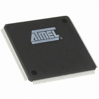
AT91M63200-25AI
Manufacturer Part Number
AT91M63200-25AI
Description
IC ARM7 MCU 176 TQFP
Manufacturer
Atmel
Series
AT91SAMr
Datasheets
1.AT91M43300-25CI.pdf
(21 pages)
2.AT91M43300-25CI.pdf
(5 pages)
3.AT91M63200-25AI.pdf
(12 pages)
4.AT91M63200-25AI.pdf
(153 pages)
Specifications of AT91M63200-25AI
Core Processor
ARM7
Core Size
16/32-Bit
Speed
25MHz
Connectivity
EBI/EMI, SPI, UART/USART
Peripherals
POR, WDT
Number Of I /o
58
Program Memory Type
OTP
Ram Size
2K x 8
Voltage - Supply (vcc/vdd)
1.8 V ~ 3.6 V
Oscillator Type
External
Operating Temperature
-40°C ~ 85°C
Package / Case
176-TQFP, 176-VQFP
Lead Free Status / RoHS Status
Contains lead / RoHS non-compliant
Eeprom Size
-
Program Memory Size
-
Data Converters
-
Available stocks
Company
Part Number
Manufacturer
Quantity
Price


Read Protocols
The EBI provides two alternative protocols for external
memory read access: standard and early read. The differ-
ence between the two protocols lies in the timing of the
NRD (read cycle) waveform.
The protocol is selected by the DRP field in EBI_MCR
(Memory Control Register) and is valid for all memory
devices. Standard read protocol is the default protocol after
reset.
Note: In the following waveforms and descriptions, NRD
represents NRD and NOE since the two signals have the
same waveform. Likewise, NWE represents NWE, NWR0
and NWR1 unless NWR0 and NWR1 are otherwise repre-
sented. ADDR represents A0-A23 and/or A1-A23.
Standard Read Protocol
Standard read protocol implements a read cycle in which
NRD and NWE are similar. Both are active during the sec-
ond half of the clock cycle. The first half of the clock cycle
allows time to ensure completion of the previous access as
well as the output of address and NCS before the read
cycle begins.
During a standard read protocol external memory access,
NCS is set low and ADDR is valid at the beginning of the
access while NRD goes low only in the second half of the
master clock cycle to avoid bus conflict (see Figure 13).
NWE is the same in both protocols. NWE always goes low
in the second half of the master clock cycle (see Figure 14).
Early Read Protocol
Early read protocol provides more time for a read access
from the memory by asserting NRD at the beginning of the
clock cycle. In the case of successive read cycles in the
same memory, NRD remains active continuously. Since a
read cycle normally limits the speed of operation of the
external memory system, early read protocol can allow a
faster clock frequency to be used. However, an extra wait
state is required in some cases to avoid contentions on the
external bus.
Early Read Wait State
In early read protocol, an early read wait state is automati-
cally inserted when an external write cycle is followed by a
read cycle to allow time for the write cycle to end before the
subsequent read cycle begins (see Figure 15). This wait
state is generated in addition to any other programmed wait
states (i.e. data float wait).
No wait state is added when a read cycle is followed by a
write cycle, between consecutive accesses of the same
type or between external and internal memory accesses.
Early read wait states affect the external bus only. They do
not affect internal bus timing.
Figure 13. Standard Read Protocol
Figure 14. Early Read Protocol
Figure 15. Early Read Wait State
ADDR
MCKI
NWE
NRD
or
NCS
or
ADDR
MCKI
ADDR
NWE
MCKI
NCS
NRD
NWE
NRD
NCS
write cycle
AT91M63200
early read wait
read cycle
15
Related parts for AT91M63200-25AI
Image
Part Number
Description
Manufacturer
Datasheet
Request
R

Part Number:
Description:
DEV KIT FOR AVR/AVR32
Manufacturer:
Atmel
Datasheet:

Part Number:
Description:
INTERVAL AND WIPE/WASH WIPER CONTROL IC WITH DELAY
Manufacturer:
ATMEL Corporation
Datasheet:
Part Number:
Description:
Low-Voltage Voice-Switched IC for Hands-Free Operation
Manufacturer:
ATMEL Corporation
Datasheet:
Part Number:
Description:
MONOLITHIC INTEGRATED FEATUREPHONE CIRCUIT
Manufacturer:
ATMEL Corporation
Datasheet:
Part Number:
Description:
AM-FM Receiver IC U4255BM-M
Manufacturer:
ATMEL Corporation
Datasheet:
Part Number:
Description:
Monolithic Integrated Feature Phone Circuit
Manufacturer:
ATMEL Corporation
Datasheet:
Part Number:
Description:
Multistandard Video-IF and Quasi Parallel Sound Processing
Manufacturer:
ATMEL Corporation
Datasheet:
Part Number:
Description:
High-performance EE PLD
Manufacturer:
ATMEL Corporation
Datasheet:
Part Number:
Description:
8-bit Flash Microcontroller
Manufacturer:
ATMEL Corporation
Datasheet:
Part Number:
Description:
2-Wire Serial EEPROM
Manufacturer:
ATMEL Corporation
Datasheet: