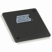
AT91M63200-25AI Atmel, AT91M63200-25AI Datasheet - Page 13

AT91M63200-25AI
Manufacturer Part Number
AT91M63200-25AI
Description
IC ARM7 MCU 176 TQFP
Manufacturer
Atmel
Series
AT91SAMr
Datasheets
1.AT91M43300-25CI.pdf
(21 pages)
2.AT91M43300-25CI.pdf
(5 pages)
3.AT91M63200-25AI.pdf
(12 pages)
4.AT91M63200-25AI.pdf
(153 pages)
Specifications of AT91M63200-25AI
Core Processor
ARM7
Core Size
16/32-Bit
Speed
25MHz
Connectivity
EBI/EMI, SPI, UART/USART
Peripherals
POR, WDT
Number Of I /o
58
Program Memory Type
OTP
Ram Size
2K x 8
Voltage - Supply (vcc/vdd)
1.8 V ~ 3.6 V
Oscillator Type
External
Operating Temperature
-40°C ~ 85°C
Package / Case
176-TQFP, 176-VQFP
Lead Free Status / RoHS Status
Contains lead / RoHS non-compliant
Eeprom Size
-
Program Memory Size
-
Data Converters
-
Available stocks
Company
Part Number
Manufacturer
Quantity
Price
- AT91M43300-25CI PDF datasheet
- AT91M43300-25CI PDF datasheet #2
- AT91M63200-25AI PDF datasheet #3
- AT91M63200-25AI PDF datasheet #4
- Current page: 13 of 153
- Download datasheet (3Mb)
Data Bus Width
A data bus width of 8 or 16 bits can be selected for each
chip select. This option is controlled by the DBW field in the
EBI_CSR (Chip Select Register) for the corresponding chip
select.
Figure 8 shows how to connect a 512K x 8-bit memory on
NCS2.
Figure 8. Memory Connection for an 8-bit Data Bus
Figure 9 shows how to connect a 512K x 16-bit memory on
NCS2.
Figure 9. Memory Connection for a 16-bit Data Bus
EBI
EBI
D8 - D15
A1 - A19
D8 - D15
A1 - A18
D0 - D7
D0 - D7
NWR1
NWR0
NCS2
NCS2
NWE
NOE
NUB
NRD
NLB
A0
D0 - D7
D8 - D15
A0 - A18
Low Byte Enable
High Byte Enable
Write Enable
Output Enable
Memory Enable
D0 - D7
A1 - A18
A0
Write Enable
Output Enable
Memory Enable
Byte Write or Byte Select Access
Each chip select with a 16-bit data bus can operate with
one of two different types of write access:
•
•
This option is controlled by the BAT field in the EBI_CSR
(Chip Select Register) for the corresponding chip select.
Byte Write access is used to connect 2 x 8-bit devices as a
16-bit memory page.
•
•
•
•
Figure 10 shows how to connect two 512K x 8-bit devices
in parallel on NCS2.
Figure 10. Memory Connection for 2 x 8-bit Data Buses
Byte Write access supports two byte-write and a single
read signal.
Byte Select access selects upper and/or lower byte with
two byte-select lines, and separate read and write
signals.
The signal A0/NLB is not used.
The signal NWR1/NUB is used as NWR1 and enables
upper byte writes.
The signal NWR0/NWE is used as NWR0 and enables
lower byte writes.
The signal NRD/NOE is used as NRD and enables half-
word and byte reads.
EBI
D8 - D15
A1 - A19
D0 - D7
NWR1
NWR0
NCS2
NRD
A0
AT91M63200
D0 - D7
A0 - A18
Write Enable
Read Enable
Memory Enable
D8 - D15
A0 - A18
Write Enable
Read Enable
Memory Enable
13
Related parts for AT91M63200-25AI
Image
Part Number
Description
Manufacturer
Datasheet
Request
R

Part Number:
Description:
DEV KIT FOR AVR/AVR32
Manufacturer:
Atmel
Datasheet:

Part Number:
Description:
INTERVAL AND WIPE/WASH WIPER CONTROL IC WITH DELAY
Manufacturer:
ATMEL Corporation
Datasheet:

Part Number:
Description:
Low-Voltage Voice-Switched IC for Hands-Free Operation
Manufacturer:
ATMEL Corporation
Datasheet:

Part Number:
Description:
MONOLITHIC INTEGRATED FEATUREPHONE CIRCUIT
Manufacturer:
ATMEL Corporation
Datasheet:

Part Number:
Description:
AM-FM Receiver IC U4255BM-M
Manufacturer:
ATMEL Corporation
Datasheet:

Part Number:
Description:
Monolithic Integrated Feature Phone Circuit
Manufacturer:
ATMEL Corporation
Datasheet:

Part Number:
Description:
Multistandard Video-IF and Quasi Parallel Sound Processing
Manufacturer:
ATMEL Corporation
Datasheet:

Part Number:
Description:
High-performance EE PLD
Manufacturer:
ATMEL Corporation
Datasheet:

Part Number:
Description:
8-bit Flash Microcontroller
Manufacturer:
ATMEL Corporation
Datasheet:

Part Number:
Description:
2-Wire Serial EEPROM
Manufacturer:
ATMEL Corporation
Datasheet:


