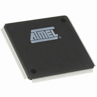
AT91M63200-25AI Atmel, AT91M63200-25AI Datasheet - Page 14

AT91M63200-25AI
Manufacturer Part Number
AT91M63200-25AI
Description
IC ARM7 MCU 176 TQFP
Manufacturer
Atmel
Series
AT91SAMr
Datasheets
1.AT91M43300-25CI.pdf
(21 pages)
2.AT91M43300-25CI.pdf
(5 pages)
3.AT91M63200-25AI.pdf
(12 pages)
4.AT91M63200-25AI.pdf
(153 pages)
Specifications of AT91M63200-25AI
Core Processor
ARM7
Core Size
16/32-Bit
Speed
25MHz
Connectivity
EBI/EMI, SPI, UART/USART
Peripherals
POR, WDT
Number Of I /o
58
Program Memory Type
OTP
Ram Size
2K x 8
Voltage - Supply (vcc/vdd)
1.8 V ~ 3.6 V
Oscillator Type
External
Operating Temperature
-40°C ~ 85°C
Package / Case
176-TQFP, 176-VQFP
Lead Free Status / RoHS Status
Contains lead / RoHS non-compliant
Eeprom Size
-
Program Memory Size
-
Data Converters
-
Available stocks
Company
Part Number
Manufacturer
Quantity
Price
Byte Select access is used to connect 16-bit devices in a
memory page.
•
•
•
•
Figure 11 shows how to connect a 16-bit device with byte
and half-word access (e.g. 16-bit SRAM) on NCS2.
Figure 11. Connection for a 16-bit Data Bus with Byte and
Half-word Access
Figure 12 shows how to connect a 16-bit device without
byte access (e.g. Flash) on NCS2.
Figure 12. Connection for a 16-bit Data Bus without Byte
Write Capability
14
EBI
EBI
The signal A0/NLB is used as NLB and enables the
lower byte for both read and write operations.
The signal NWR1/NUB is used as NUB and enables the
upper byte for both read and write operations.
The signal NWR0/NWE is used as NWE and enables
writing for byte or half-word.
The signal NRD/NOE is used as NOE and enables
reading for byte or half-word.
D8 - D15
D8 - D15
A1 - A19
A1 - A19
D0 - D7
D0 - D7
NCS2
NCS2
NWE
NWE
NOE
NOE
NUB
NUB
NLB
NLB
AT91M63200
D0 - D7
D8 - D15
A0 - A18
Write Enable
Output Enable
Memory Enable
D0 - D7
D8 - D15
A0 - A18
Low Byte Enable
High Byte Enable
Write Enable
Output Enable
Memory Enable
Boot
Conventional program operation requires RAM memory at
page zero to support dynamic exception vectors. However,
it is necessary to boot from nonvolatile memory at page
zero.
When the AT91M63200 is reset, the memory map is modi-
fied to place NVM at page zero. The on-chip RAM is
remapped to address 0x00300000 and either on-chip 32-bit
NVM or off-chip 8/16-bit NVM is remapped to address
0x00000000. The off-chip NVM is selected on NCS0.
The boot memory type is selected by the BMS pin when
NRST is active (see “Boot Mode Select” on page 9).
Watchdog reset does not change the boot memory selec-
tion but does perform a full reboot from the previously-
selected memory.
The memory map is returned to its conventional configura-
tion by writing 1 to the RCB bit of the EBI_RCR (Remap
Control Register). This cancels the remapping and enables
normal operation of the EBI, as programmed (see
page 34). It is not possible to remap the memory by writing
0 to the RCB bit in EBI_RCR.
During boot, the number of external devices (number of
active chip selects) and their configurations must be pro-
grammed as described in the EBI user interface (see
page 31). The chip select addresses which are pro-
grammed take effect when memory remapping is can-
celled. Only NCS0 is active while the memory is remapped.
Wait states take effect immediately when they are pro-
grammed to allow boot program execution to be optimized.


