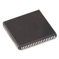
HD64F3337YCP16V Renesas Electronics America, HD64F3337YCP16V Datasheet - Page 568

HD64F3337YCP16V
Manufacturer Part Number
HD64F3337YCP16V
Description
MCU 3/5V 60K PB-FREE 84-PLCC
Manufacturer
Renesas Electronics America
Series
H8® H8/300r
Specifications of HD64F3337YCP16V
Core Size
8-Bit
Program Memory Size
60KB (60K x 8)
Oscillator Type
Internal
Core Processor
H8/300
Speed
16MHz
Connectivity
Host Interface, I²C, SCI
Peripherals
POR, PWM, WDT
Number Of I /o
74
Program Memory Type
FLASH
Ram Size
2K x 8
Voltage - Supply (vcc/vdd)
4.5 V ~ 5.5 V
Data Converters
A/D 8x10b; D/A 2x8b
Operating Temperature
-20°C ~ 75°C
Package / Case
84-PLCC
No. Of I/o's
74
Ram Memory Size
1KB
Cpu Speed
16MHz
No. Of Timers
6
No. Of Pwm Channels
2
Digital Ic Case Style
PLCC
Controller Family/series
H8/300
Rohs Compliant
Yes
Lead Free Status / RoHS Status
Lead free / RoHS Compliant
Eeprom Size
-
Lead Free Status / RoHS Status
Lead free / RoHS Compliant, Lead free / RoHS Compliant
Available stocks
Company
Part Number
Manufacturer
Quantity
Price
Company:
Part Number:
HD64F3337YCP16V
Manufacturer:
COILMASTER
Quantity:
30 000
Company:
Part Number:
HD64F3337YCP16V
Manufacturer:
Renesas Electronics America
Quantity:
10 000
- Current page: 568 of 749
- Download datasheet (4Mb)
21.6
Read these precautions before using writer mode, on-board programming mode, or flash memory
emulation by RAM.
(1) Program with the specified voltage and timing.
When using a PROM programmer to reprogram the on-chip flash memory in the single-power-
supply model (S-mask model), use a PROM programmer that supports the Hitachi microcomputer
device type with 64-kbyte on-chip flash memory (5.0 V programming voltage), do not set the
programmer to the HN28F101 3.3 V programming voltage and only use the specified socket
adapter. Failure to observe these precautions may result in damage to the device.
(2) Before programming, check that the chip is correctly mounted in the PROM
programmer.
Overcurrent damage to the device can occur if the index marks on the PROM programmer socket,
socket adapter, and chip are not correctly aligned.
(3) Don’t touch the socket adapter or chip while programming.
Touching either of these can cause contact faults and write errors.
(4) Set H'FF as the PROM programmer buffer data for addresses H'F780 to H'1FFFF.
The H8/3337SF PROM size is 60 kbytes. Addresses H'F780 to H'1FFFF always read H'FF, so if
H'FF is not specified as programmer data, a block error will occur.
(5) Use the recommended algorithms for programming and erasing flash memory.
These algorithms are designed to program and erase without subjecting the device to voltage stress
and without sacrificing the reliability of programmed data.
Before setting the program (P) or erase (E) bit in flash memory control register 1 (FLMCR1), set
the watchdog timer to ensure that the P or E bit does not remain set for more than the specified
time.
(6) For details on interrupt handling while flash memory is being programmed or erased,
see section 21.4.6, Interrupt Handling during Flash Memory Programming and Erasing.
(7) Cautions on Accessing Flash Memory Control Registers
1. Flash memory control register access state in each operating mode
536
The H8/3337SF has flash memory control registers located at addresses H'FF80 (FLMCR1),
H'FF81 (FLMCR2), and H'FF83 (EBR2). These registers can only be accessed when the
FLSHE bit is set to 1 in the wait-state control register (WSCR).
Table 21.22 shows the area accessed for the above addresses in each mode, when FLSHE = 0
and when FLSHE = 1.
Flash Memory Programming and Erasing Precautions
Related parts for HD64F3337YCP16V
Image
Part Number
Description
Manufacturer
Datasheet
Request
R

Part Number:
Description:
KIT STARTER FOR M16C/29
Manufacturer:
Renesas Electronics America
Datasheet:

Part Number:
Description:
KIT STARTER FOR R8C/2D
Manufacturer:
Renesas Electronics America
Datasheet:

Part Number:
Description:
R0K33062P STARTER KIT
Manufacturer:
Renesas Electronics America
Datasheet:

Part Number:
Description:
KIT STARTER FOR R8C/23 E8A
Manufacturer:
Renesas Electronics America
Datasheet:

Part Number:
Description:
KIT STARTER FOR R8C/25
Manufacturer:
Renesas Electronics America
Datasheet:

Part Number:
Description:
KIT STARTER H8S2456 SHARPE DSPLY
Manufacturer:
Renesas Electronics America
Datasheet:

Part Number:
Description:
KIT STARTER FOR R8C38C
Manufacturer:
Renesas Electronics America
Datasheet:

Part Number:
Description:
KIT STARTER FOR R8C35C
Manufacturer:
Renesas Electronics America
Datasheet:

Part Number:
Description:
KIT STARTER FOR R8CL3AC+LCD APPS
Manufacturer:
Renesas Electronics America
Datasheet:

Part Number:
Description:
KIT STARTER FOR RX610
Manufacturer:
Renesas Electronics America
Datasheet:

Part Number:
Description:
KIT STARTER FOR R32C/118
Manufacturer:
Renesas Electronics America
Datasheet:

Part Number:
Description:
KIT DEV RSK-R8C/26-29
Manufacturer:
Renesas Electronics America
Datasheet:

Part Number:
Description:
KIT STARTER FOR SH7124
Manufacturer:
Renesas Electronics America
Datasheet:

Part Number:
Description:
KIT STARTER FOR H8SX/1622
Manufacturer:
Renesas Electronics America
Datasheet:

Part Number:
Description:
KIT DEV FOR SH7203
Manufacturer:
Renesas Electronics America
Datasheet:


