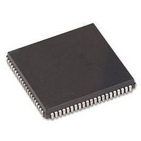
HD64F3337YCP16V Renesas Electronics America, HD64F3337YCP16V Datasheet - Page 390

HD64F3337YCP16V
Manufacturer Part Number
HD64F3337YCP16V
Description
MCU 3/5V 60K PB-FREE 84-PLCC
Manufacturer
Renesas Electronics America
Series
H8® H8/300r
Specifications of HD64F3337YCP16V
Core Size
8-Bit
Program Memory Size
60KB (60K x 8)
Oscillator Type
Internal
Core Processor
H8/300
Speed
16MHz
Connectivity
Host Interface, I²C, SCI
Peripherals
POR, PWM, WDT
Number Of I /o
74
Program Memory Type
FLASH
Ram Size
2K x 8
Voltage - Supply (vcc/vdd)
4.5 V ~ 5.5 V
Data Converters
A/D 8x10b; D/A 2x8b
Operating Temperature
-20°C ~ 75°C
Package / Case
84-PLCC
No. Of I/o's
74
Ram Memory Size
1KB
Cpu Speed
16MHz
No. Of Timers
6
No. Of Pwm Channels
2
Digital Ic Case Style
PLCC
Controller Family/series
H8/300
Rohs Compliant
Yes
Lead Free Status / RoHS Status
Lead free / RoHS Compliant
Eeprom Size
-
Lead Free Status / RoHS Status
Lead free / RoHS Compliant, Lead free / RoHS Compliant
Available stocks
Company
Part Number
Manufacturer
Quantity
Price
Company:
Part Number:
HD64F3337YCP16V
Manufacturer:
COILMASTER
Quantity:
30 000
Company:
Part Number:
HD64F3337YCP16V
Manufacturer:
Renesas Electronics America
Quantity:
10 000
- Current page: 390 of 749
- Download datasheet (4Mb)
16.3
The D/A converter module has two built-in D/A converter circuits that can operate independently.
D/A conversion is performed continuously whenever enabled by the D/A control register. When a
new value is written in DADR0 or DADR1, conversion of the new value begins immediately. The
converted result is output by setting the DAOE0 or DAOE1 bit to 1.
An example of conversion on channel 0 is given next. Figure 16.2 shows the timing.
1. Software writes the data to be converted in DADR0.
2. D/A conversion begins when the DAOE0 bit in DACR is set to 1. After a conversion delay,
3. If a new value is written in DADR0, conversion begins immediately. Output of the converted
4. When the DAOE0 bit is cleared to 0, DA0 becomes an input pin.
358
ø
Address
DADR0
DAOE0
DA0
t
DCONV
analog output appears at the DA0 pin. The output value is AV
This output continues until a new value is written in DADR0 or the DAOE0 bit is cleared to 0.
result begins after the conversion delay time.
: D/A conversion time
Operation
DADR0
write cycle
High-impedance state
DACR
write cycle
Figure 16.2 D/A Conversion (Example)
Conversion data (1)
t
DCONV
Conversion result (1)
DADR0
write cycle
CC
(DADR0 value)/256.
t
DCONV
Conversion data (2)
Conversion result (2)
DACR
write cycle
Related parts for HD64F3337YCP16V
Image
Part Number
Description
Manufacturer
Datasheet
Request
R

Part Number:
Description:
KIT STARTER FOR M16C/29
Manufacturer:
Renesas Electronics America
Datasheet:

Part Number:
Description:
KIT STARTER FOR R8C/2D
Manufacturer:
Renesas Electronics America
Datasheet:

Part Number:
Description:
R0K33062P STARTER KIT
Manufacturer:
Renesas Electronics America
Datasheet:

Part Number:
Description:
KIT STARTER FOR R8C/23 E8A
Manufacturer:
Renesas Electronics America
Datasheet:

Part Number:
Description:
KIT STARTER FOR R8C/25
Manufacturer:
Renesas Electronics America
Datasheet:

Part Number:
Description:
KIT STARTER H8S2456 SHARPE DSPLY
Manufacturer:
Renesas Electronics America
Datasheet:

Part Number:
Description:
KIT STARTER FOR R8C38C
Manufacturer:
Renesas Electronics America
Datasheet:

Part Number:
Description:
KIT STARTER FOR R8C35C
Manufacturer:
Renesas Electronics America
Datasheet:

Part Number:
Description:
KIT STARTER FOR R8CL3AC+LCD APPS
Manufacturer:
Renesas Electronics America
Datasheet:

Part Number:
Description:
KIT STARTER FOR RX610
Manufacturer:
Renesas Electronics America
Datasheet:

Part Number:
Description:
KIT STARTER FOR R32C/118
Manufacturer:
Renesas Electronics America
Datasheet:

Part Number:
Description:
KIT DEV RSK-R8C/26-29
Manufacturer:
Renesas Electronics America
Datasheet:

Part Number:
Description:
KIT STARTER FOR SH7124
Manufacturer:
Renesas Electronics America
Datasheet:

Part Number:
Description:
KIT STARTER FOR H8SX/1622
Manufacturer:
Renesas Electronics America
Datasheet:

Part Number:
Description:
KIT DEV FOR SH7203
Manufacturer:
Renesas Electronics America
Datasheet:


