AT90CAN128-15AZ Atmel, AT90CAN128-15AZ Datasheet - Page 351
AT90CAN128-15AZ
Manufacturer Part Number
AT90CAN128-15AZ
Description
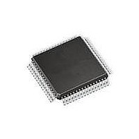
MCU AVR 128K FLASH 15MHZ 64TQFP
Manufacturer
Atmel
Series
AVR® 90CANr
Specifications of AT90CAN128-15AZ
Package / Case
64-TQFP, 64-VQFP
Voltage - Supply (vcc/vdd)
2.7 V ~ 5.5 V
Operating Temperature
-40°C ~ 125°C
Speed
16MHz
Number Of I /o
53
Eeprom Size
4K x 8
Core Processor
AVR
Program Memory Type
FLASH
Ram Size
4K x 8
Program Memory Size
128KB (128K x 8)
Data Converters
A/D 8x10b
Oscillator Type
Internal
Peripherals
Brown-out Detect/Reset, POR, PWM, WDT
Connectivity
CAN, I²C, SPI, UART/USART
Core Size
8-Bit
Processor Series
AT90CANx
Core
AVR8
Data Bus Width
8 bit
Data Ram Size
4 KB
Interface Type
CAN, SPI, UART
Maximum Clock Frequency
16 MHz
Number Of Programmable I/os
53
Number Of Timers
4
Maximum Operating Temperature
+ 125 C
Mounting Style
SMD/SMT
3rd Party Development Tools
EWAVR, EWAVR-BL
Development Tools By Supplier
ATAVRDRAGON, ATSTK500, ATSTK600, ATAVRISP2, ATDVK90CAN1, ATADAPCAN01
Minimum Operating Temperature
- 40 C
On-chip Adc
10 bit, 8 Channel
Cpu Family
90C
Device Core
AVR
Device Core Size
8b
Frequency (max)
16MHz
Total Internal Ram Size
4KB
# I/os (max)
53
Number Of Timers - General Purpose
4
Operating Supply Voltage (typ)
3.3/5V
Operating Supply Voltage (max)
5.5V
Operating Supply Voltage (min)
2.7V
Instruction Set Architecture
RISC
Operating Temp Range
-40C to 125C
Operating Temperature Classification
Automotive
Mounting
Surface Mount
Pin Count
64
Package Type
TQFP
Lead Free Status / RoHS Status
Lead free / RoHS Compliant
Available stocks
Company
Part Number
Manufacturer
Quantity
Price
Company:

Part Number:
AT90CAN128-15AZ
Manufacturer:
SAMSUNG
Quantity:
1 001
Company:
Part Number:
AT90CAN128-15AZ
Manufacturer:
ATMEL
Quantity:
1 000
Part Number:
AT90CAN128-15AZ
Manufacturer:
ATMEL/爱特梅尔
Quantity:
20 000


Table 25-15. Serial Programming Instruction Set
7679H–CAN–08/08
Instruction
Programming
Enable
Chip Erase
Read
Program Memory
Load
Program Memory
Page
Write
Program Memory
Page
Read
EEPROM Memory
Write
EEPROM Memory
Set
a = address high bits, b = address low bits, H = 0 - Low byte, 1 - High Byte, o = data out, i = data in, x = don’t care
1010 1100 0101 0011 xxxx xxxx xxxx xxxx Enable Serial Programming after RESET goes low.
1010 1100 100x xxxx xxxx xxxx xxxx xxxx Chip Erase EEPROM and Flash.
0010 H000 aaaa aaaa bbbb bbbb oooo oooo
0100 H000 000x xxxx xbbb bbbb iiii iiii
0100 1100 aaaa aaaa bxxx xxxx xxxx xxxx Write Program Memory Page at address a:b.
1010 0000 000x aaaa bbbb bbbb oooo oooo Read data o from EEPROM memory at address a:b.
1100 0000 000x aaaa bbbb bbbb iiii iiii Write data i to EEPROM memory at address a:b.
Byte 1
are meant to contain 0xFF, can be skipped. This does not apply if the EEPROM is re-pro-
grammed without chip erasing the device. In this case, data polling cannot be used for the value
0xFF, and the user will have to wait at least t
Table 25-14
Table 25-14. Minimum Wait Delay Before Writing the Next Flash or EEPROM Location
Figure 25-8. Serial Programming Waveforms
Symbol
t
t
t
t
WD_FUSE
WD_FLASH
WD_EEPROM
WD_ERASE
SERIAL DA TA OUTPUT
SERIAL CLOCK INPUT
Byte 2
Instruction Format
SERIAL DA TA INPUT
for t
(2)
WD_EEPROM
(MISO-PDO)
(MOSI-PDI)
Sample
(SCK)
Byte 3
value.
(1)
MSB
MSB
Byte4
WD_EEPROM
Operation
Read H (high or low) data o from Program memory at
word address a:b.
Write H (high or low) data i to Program Memory page
at word address b. Data low byte must be loaded
before Data high byte is applied within the same
address.
Minimum Wait Delay
(1)
before programming the next byte. See
AT90CAN32/64/128
4.5 ms
4.5 ms
9.0 ms
9.0 ms
LSB
LSB
351
Related parts for AT90CAN128-15AZ
Image
Part Number
Description
Manufacturer
Datasheet
Request
R

Part Number:
Description:
DEV KIT FOR AVR/AVR32
Manufacturer:
Atmel
Datasheet:

Part Number:
Description:
INTERVAL AND WIPE/WASH WIPER CONTROL IC WITH DELAY
Manufacturer:
ATMEL Corporation
Datasheet:
Part Number:
Description:
Low-Voltage Voice-Switched IC for Hands-Free Operation
Manufacturer:
ATMEL Corporation
Datasheet:
Part Number:
Description:
MONOLITHIC INTEGRATED FEATUREPHONE CIRCUIT
Manufacturer:
ATMEL Corporation
Datasheet:
Part Number:
Description:
AM-FM Receiver IC U4255BM-M
Manufacturer:
ATMEL Corporation
Datasheet:
Part Number:
Description:
Monolithic Integrated Feature Phone Circuit
Manufacturer:
ATMEL Corporation
Datasheet:
Part Number:
Description:
Multistandard Video-IF and Quasi Parallel Sound Processing
Manufacturer:
ATMEL Corporation
Datasheet:
Part Number:
Description:
High-performance EE PLD
Manufacturer:
ATMEL Corporation
Datasheet:
Part Number:
Description:
8-bit Flash Microcontroller
Manufacturer:
ATMEL Corporation
Datasheet:
Part Number:
Description:
2-Wire Serial EEPROM
Manufacturer:
ATMEL Corporation
Datasheet: