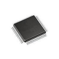
AT90CAN128-15AZ Atmel, AT90CAN128-15AZ Datasheet - Page 293

AT90CAN128-15AZ
Manufacturer Part Number
AT90CAN128-15AZ
Description
MCU AVR 128K FLASH 15MHZ 64TQFP
Manufacturer
Atmel
Series
AVR® 90CANr
Specifications of AT90CAN128-15AZ
Package / Case
64-TQFP, 64-VQFP
Voltage - Supply (vcc/vdd)
2.7 V ~ 5.5 V
Operating Temperature
-40°C ~ 125°C
Speed
16MHz
Number Of I /o
53
Eeprom Size
4K x 8
Core Processor
AVR
Program Memory Type
FLASH
Ram Size
4K x 8
Program Memory Size
128KB (128K x 8)
Data Converters
A/D 8x10b
Oscillator Type
Internal
Peripherals
Brown-out Detect/Reset, POR, PWM, WDT
Connectivity
CAN, I²C, SPI, UART/USART
Core Size
8-Bit
Processor Series
AT90CANx
Core
AVR8
Data Bus Width
8 bit
Data Ram Size
4 KB
Interface Type
CAN, SPI, UART
Maximum Clock Frequency
16 MHz
Number Of Programmable I/os
53
Number Of Timers
4
Maximum Operating Temperature
+ 125 C
Mounting Style
SMD/SMT
3rd Party Development Tools
EWAVR, EWAVR-BL
Development Tools By Supplier
ATAVRDRAGON, ATSTK500, ATSTK600, ATAVRISP2, ATDVK90CAN1, ATADAPCAN01
Minimum Operating Temperature
- 40 C
On-chip Adc
10 bit, 8 Channel
Cpu Family
90C
Device Core
AVR
Device Core Size
8b
Frequency (max)
16MHz
Total Internal Ram Size
4KB
# I/os (max)
53
Number Of Timers - General Purpose
4
Operating Supply Voltage (typ)
3.3/5V
Operating Supply Voltage (max)
5.5V
Operating Supply Voltage (min)
2.7V
Instruction Set Architecture
RISC
Operating Temp Range
-40C to 125C
Operating Temperature Classification
Automotive
Mounting
Surface Mount
Pin Count
64
Package Type
TQFP
Lead Free Status / RoHS Status
Lead free / RoHS Compliant
Available stocks
Company
Part Number
Manufacturer
Quantity
Price
Company:
Part Number:
AT90CAN128-15AZ
Manufacturer:
SAMSUNG
Quantity:
1 001
Company:
Part Number:
AT90CAN128-15AZ
Manufacturer:
ATMEL
Quantity:
1 000
Part Number:
AT90CAN128-15AZ
Manufacturer:
ATMEL/爱特梅尔
Quantity:
20 000
- Current page: 293 of 428
- Download datasheet (6Mb)
22. JTAG Interface and On-chip Debug System
22.1
22.2
22.3
7679H–CAN–08/08
Features
Overview
Test Access Port – TAP
•
•
•
•
•
•
The AVR IEEE std. 1149.1 compliant JTAG interface can be used for:
A brief description is given in the following sections. Detailed descriptions for Programming via
the JTAG interface, and using the Boundary-scan Chain can be found in the sections
Programming Overview” on page 352
respectively. The On-chip Debug support is considered being private JTAG instructions, and dis-
tributed within ATMEL and to selected third party vendors only.
Figure 22-1
TAP Controller is a state machine controlled by the TCK and TMS signals. The TAP Controller
selects either the JTAG Instruction Register or one of several Data Registers as the scan chain
(Shift Register) between the TDI – input and TDO – output. The Instruction Register holds JTAG
instructions controlling the behavior of a Data Register.
The ID-Register (IDentifier Register), Bypass Register, and the Boundary-scan Chain are the
Data Registers used for board-level testing. The JTAG Programming Interface (actually consist-
ing of several physical and virtual Data Registers) is used for serial programming via the JTAG
interface. The Internal Scan Chain and Break Point Scan Chain are used for On-chip debugging
only.
The JTAG interface is accessed through four of the AVR’s pins. In JTAG terminology, these pins
constitute the Test Access Port – TAP. These pins are:
• Testing PCBs by using the JTAG Boundary-scan capability
• Programming the non-volatile memories, Fuses and Lock bits
• On-chip debugging
• TMS: Test mode select. This pin is used for navigating through the TAP-controller state
JTAG (IEEE std. 1149.1 Compliant) Interface
Boundary-scan Capabilities According to the IEEE std. 1149.1 (JTAG) Standard
Debugger Access to:
Extensive On-chip Debug Support for Break Conditions, Including
Programming of Flash, EEPROM, Fuses, and Lock Bits through the JTAG Interface
On-chip Debugging Supported by AVR Studio
machine.
– All Internal Peripheral Units
– Internal and External RAM
– The Internal Register File
– Program Counter
– EEPROM and Flash Memories
– AVR Break Instruction
– Break on Change of Program Memory Flow
– Single Step Break
– Program Memory Break Points on Single Address or Address Range
– Data Memory Break Points on Single Address or Address Range
shows a block diagram of the JTAG interface and the On-chip Debug system. The
and
“Boundary-scan IEEE 1149.1 (JTAG)” on page
®
AT90CAN32/64/128
“JTAG
300,
293
Related parts for AT90CAN128-15AZ
Image
Part Number
Description
Manufacturer
Datasheet
Request
R

Part Number:
Description:
DEV KIT FOR AVR/AVR32
Manufacturer:
Atmel
Datasheet:

Part Number:
Description:
INTERVAL AND WIPE/WASH WIPER CONTROL IC WITH DELAY
Manufacturer:
ATMEL Corporation
Datasheet:

Part Number:
Description:
Low-Voltage Voice-Switched IC for Hands-Free Operation
Manufacturer:
ATMEL Corporation
Datasheet:

Part Number:
Description:
MONOLITHIC INTEGRATED FEATUREPHONE CIRCUIT
Manufacturer:
ATMEL Corporation
Datasheet:

Part Number:
Description:
AM-FM Receiver IC U4255BM-M
Manufacturer:
ATMEL Corporation
Datasheet:

Part Number:
Description:
Monolithic Integrated Feature Phone Circuit
Manufacturer:
ATMEL Corporation
Datasheet:

Part Number:
Description:
Multistandard Video-IF and Quasi Parallel Sound Processing
Manufacturer:
ATMEL Corporation
Datasheet:

Part Number:
Description:
High-performance EE PLD
Manufacturer:
ATMEL Corporation
Datasheet:

Part Number:
Description:
8-bit Flash Microcontroller
Manufacturer:
ATMEL Corporation
Datasheet:

Part Number:
Description:
2-Wire Serial EEPROM
Manufacturer:
ATMEL Corporation
Datasheet:


