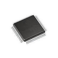
AT90CAN128-15AZ Atmel, AT90CAN128-15AZ Datasheet - Page 149

AT90CAN128-15AZ
Manufacturer Part Number
AT90CAN128-15AZ
Description
MCU AVR 128K FLASH 15MHZ 64TQFP
Manufacturer
Atmel
Series
AVR® 90CANr
Specifications of AT90CAN128-15AZ
Package / Case
64-TQFP, 64-VQFP
Voltage - Supply (vcc/vdd)
2.7 V ~ 5.5 V
Operating Temperature
-40°C ~ 125°C
Speed
16MHz
Number Of I /o
53
Eeprom Size
4K x 8
Core Processor
AVR
Program Memory Type
FLASH
Ram Size
4K x 8
Program Memory Size
128KB (128K x 8)
Data Converters
A/D 8x10b
Oscillator Type
Internal
Peripherals
Brown-out Detect/Reset, POR, PWM, WDT
Connectivity
CAN, I²C, SPI, UART/USART
Core Size
8-Bit
Processor Series
AT90CANx
Core
AVR8
Data Bus Width
8 bit
Data Ram Size
4 KB
Interface Type
CAN, SPI, UART
Maximum Clock Frequency
16 MHz
Number Of Programmable I/os
53
Number Of Timers
4
Maximum Operating Temperature
+ 125 C
Mounting Style
SMD/SMT
3rd Party Development Tools
EWAVR, EWAVR-BL
Development Tools By Supplier
ATAVRDRAGON, ATSTK500, ATSTK600, ATAVRISP2, ATDVK90CAN1, ATADAPCAN01
Minimum Operating Temperature
- 40 C
On-chip Adc
10 bit, 8 Channel
Cpu Family
90C
Device Core
AVR
Device Core Size
8b
Frequency (max)
16MHz
Total Internal Ram Size
4KB
# I/os (max)
53
Number Of Timers - General Purpose
4
Operating Supply Voltage (typ)
3.3/5V
Operating Supply Voltage (max)
5.5V
Operating Supply Voltage (min)
2.7V
Instruction Set Architecture
RISC
Operating Temp Range
-40C to 125C
Operating Temperature Classification
Automotive
Mounting
Surface Mount
Pin Count
64
Package Type
TQFP
Lead Free Status / RoHS Status
Lead free / RoHS Compliant
Available stocks
Company
Part Number
Manufacturer
Quantity
Price
Company:
Part Number:
AT90CAN128-15AZ
Manufacturer:
SAMSUNG
Quantity:
1 001
Company:
Part Number:
AT90CAN128-15AZ
Manufacturer:
ATMEL
Quantity:
1 000
Part Number:
AT90CAN128-15AZ
Manufacturer:
ATMEL/爱特梅尔
Quantity:
20 000
- Current page: 149 of 428
- Download datasheet (6Mb)
14.5.1
14.5.2
14.5.3
14.6
7679H–CAN–08/08
Compare Match Output Unit
Force Output Compare
Compare Match Blocking by TCNT2 Write
Using the Output Compare Unit
Register to either top or bottom of the counting sequence. The synchronization prevents the
occurrence of odd-length, non-symmetrical PWM pulses, thereby making the output glitch-free.
The OCR2A Register access may seem complex, but this is not case. When the double buffer-
ing is enabled, the CPU has access to the OCR2A Buffer Register, and if double buffering is
disabled the CPU will access the OCR2A directly.
In non-PWM waveform generation modes, the match output of the comparator can be forced by
writing a one to the Force Output Compare (FOC2A) bit. Forcing compare match will not set the
OCF2A flag or reload/clear the timer, but the OC2A pin will be updated as if a real compare
match had occurred (the COM2A1:0 bits settings define whether the OC2A pin is set, cleared or
toggled).
All CPU write operations to the TCNT2 Register will block any compare match that occurs in the
next timer clock cycle, even when the timer is stopped. This feature allows OCR2A to be initial-
ized to the same value as TCNT2 without triggering an interrupt when the Timer/Counter clock is
enabled.
Since writing TCNT2 in any mode of operation will block all compare matches for one timer clock
cycle, there are risks involved when changing TCNT2 when using the Output Compare channel,
independently of whether the Timer/Counter is running or not. If the value written to TCNT2
equals the OCR2A value, the compare match will be missed, resulting in incorrect waveform
generation. Similarly, do not write the TCNT2 value equal to BOTTOM when the counter is
downcounting.
The setup of the OC2A should be performed before setting the Data Direction Register for the
port pin to output. The easiest way of setting the OC2A value is to use the Force Output Com-
pare (FOC2A) strobe bit in Normal mode. The OC2A Register keeps its value even when
changing between Waveform Generation modes.
Be aware that the COM2A1:0 bits are not double buffered together with the compare value.
Changing the COM2A1:0 bits will take effect immediately.
The Compare Output mode (COM2A1:0) bits have two functions. The Waveform Generator
uses the COM2A1:0 bits for defining the Output Compare (OC2A) state at the next compare
match. Also, the COM2A1:0 bits control the OC2A pin output source.
plified schematic of the logic affected by the COM2A1:0 bit setting. The I/O Registers, I/O bits,
and I/O pins in the figure are shown in bold. Only the parts of the general I/O port control regis-
ters (DDR and PORT) that are affected by the COM2A1:0 bits are shown. When referring to the
OC2A state, the reference is for the internal OC2A Register, not the OC2A pin.
AT90CAN32/64/128
Figure 14-5
shows a sim-
149
Related parts for AT90CAN128-15AZ
Image
Part Number
Description
Manufacturer
Datasheet
Request
R

Part Number:
Description:
DEV KIT FOR AVR/AVR32
Manufacturer:
Atmel
Datasheet:

Part Number:
Description:
INTERVAL AND WIPE/WASH WIPER CONTROL IC WITH DELAY
Manufacturer:
ATMEL Corporation
Datasheet:

Part Number:
Description:
Low-Voltage Voice-Switched IC for Hands-Free Operation
Manufacturer:
ATMEL Corporation
Datasheet:

Part Number:
Description:
MONOLITHIC INTEGRATED FEATUREPHONE CIRCUIT
Manufacturer:
ATMEL Corporation
Datasheet:

Part Number:
Description:
AM-FM Receiver IC U4255BM-M
Manufacturer:
ATMEL Corporation
Datasheet:

Part Number:
Description:
Monolithic Integrated Feature Phone Circuit
Manufacturer:
ATMEL Corporation
Datasheet:

Part Number:
Description:
Multistandard Video-IF and Quasi Parallel Sound Processing
Manufacturer:
ATMEL Corporation
Datasheet:

Part Number:
Description:
High-performance EE PLD
Manufacturer:
ATMEL Corporation
Datasheet:

Part Number:
Description:
8-bit Flash Microcontroller
Manufacturer:
ATMEL Corporation
Datasheet:

Part Number:
Description:
2-Wire Serial EEPROM
Manufacturer:
ATMEL Corporation
Datasheet:


