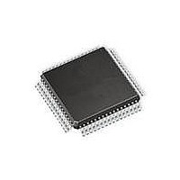
AT90CAN128-15AZ Atmel, AT90CAN128-15AZ Datasheet - Page 162

AT90CAN128-15AZ
Manufacturer Part Number
AT90CAN128-15AZ
Description
MCU AVR 128K FLASH 15MHZ 64TQFP
Manufacturer
Atmel
Series
AVR® 90CANr
Specifications of AT90CAN128-15AZ
Package / Case
64-TQFP, 64-VQFP
Voltage - Supply (vcc/vdd)
2.7 V ~ 5.5 V
Operating Temperature
-40°C ~ 125°C
Speed
16MHz
Number Of I /o
53
Eeprom Size
4K x 8
Core Processor
AVR
Program Memory Type
FLASH
Ram Size
4K x 8
Program Memory Size
128KB (128K x 8)
Data Converters
A/D 8x10b
Oscillator Type
Internal
Peripherals
Brown-out Detect/Reset, POR, PWM, WDT
Connectivity
CAN, I²C, SPI, UART/USART
Core Size
8-Bit
Processor Series
AT90CANx
Core
AVR8
Data Bus Width
8 bit
Data Ram Size
4 KB
Interface Type
CAN, SPI, UART
Maximum Clock Frequency
16 MHz
Number Of Programmable I/os
53
Number Of Timers
4
Maximum Operating Temperature
+ 125 C
Mounting Style
SMD/SMT
3rd Party Development Tools
EWAVR, EWAVR-BL
Development Tools By Supplier
ATAVRDRAGON, ATSTK500, ATSTK600, ATAVRISP2, ATDVK90CAN1, ATADAPCAN01
Minimum Operating Temperature
- 40 C
On-chip Adc
10 bit, 8 Channel
Cpu Family
90C
Device Core
AVR
Device Core Size
8b
Frequency (max)
16MHz
Total Internal Ram Size
4KB
# I/os (max)
53
Number Of Timers - General Purpose
4
Operating Supply Voltage (typ)
3.3/5V
Operating Supply Voltage (max)
5.5V
Operating Supply Voltage (min)
2.7V
Instruction Set Architecture
RISC
Operating Temp Range
-40C to 125C
Operating Temperature Classification
Automotive
Mounting
Surface Mount
Pin Count
64
Package Type
TQFP
Lead Free Status / RoHS Status
Lead free / RoHS Compliant
Available stocks
Company
Part Number
Manufacturer
Quantity
Price
Company:
Part Number:
AT90CAN128-15AZ
Manufacturer:
SAMSUNG
Quantity:
1 001
Company:
Part Number:
AT90CAN128-15AZ
Manufacturer:
ATMEL
Quantity:
1 000
Part Number:
AT90CAN128-15AZ
Manufacturer:
ATMEL/爱特梅尔
Quantity:
20 000
- Current page: 162 of 428
- Download datasheet (6Mb)
14.10.3
14.10.4
162
AT90CAN32/64/128
Timer/Counter2 Interrupt Mask Register – TIMSK2
Timer/Counter2 Interrupt Flag Register – TIFR2
• Bit 7..2 – Reserved Bits
These bits are reserved for future use.
• Bit 1 – OCIE2A: Timer/Counter2 Output Compare Match A Interrupt Enable
When the OCIE2A bit is written to one and the I-bit in the Status Register is set (one), the
Timer/Counter2 Compare Match A interrupt is enabled. The corresponding interrupt is executed
if a compare match in Timer/Counter2 occurs, i.e., when the OCF2A bit is set in the
Timer/Counter2 Interrupt Flag Register – TIFR2.
• Bit 0 – TOIE2: Timer/Counter2 Overflow Interrupt Enable
When the TOIE2 bit is written to one and the I-bit in the Status Register is set (one), the
Timer/Counter2 Overflow interrupt is enabled. The corresponding interrupt is executed if an
overflow in Timer/Counter2 occurs, i.e., when the TOV2 bit is set in the Timer/Counter2 Interrupt
Flag Register – TIFR2.
Bit
Read/Write
Initial Value
Bit
Read/Write
Initial Value
• Description of wake up from Power-save mode when the timer is clocked asynchronously:
• Reading of the TCNT2 Register shortly after wake-up from Power-save may give an incorrect
• During asynchronous operation, the synchronization of the interrupt flags for the
When the interrupt condition is met, the wake up process is started on the following cycle of
the timer clock, that is, the timer is always advanced by at least one before the processor can
read the counter value. After wake-up, the MCU is halted for four cycles, it executes the
interrupt routine, and resumes execution from the instruction following SLEEP.
result. Since TCNT2 is clocked on the asynchronous TOSC clock, reading TCNT2 must be
done through a register synchronized to the internal I/O clock domain. Synchronization takes
place for every rising TOSC1 edge. When waking up from Power-save mode, and the I/O
clock (clk
sleep) until the next rising TOSC1 edge. The phase of the TOSC clock after waking up from
Power-save mode is essentially unpredictable, as it depends on the wake-up time. The
recommended procedure for reading TCNT2 is thus as follows:
asynchronous timer takes 3 processor cycles plus one timer cycle. The timer is therefore
advanced by at least one before the processor can read the timer value causing the setting of
the interrupt flag. The Output Compare pin is changed on the timer clock and is not
synchronized to the processor clock.
a. Write any value to either of the registers OCR2A or TCCR2A.
b. Wait for the corresponding Update Busy Flag to be cleared.
c. Read TCNT2.
I/O
) again becomes active, TCNT2 will read as the previous value (before entering
R
R
7
–
0
7
–
0
R
R
6
–
0
6
–
0
R
R
5
–
0
5
–
0
R
R
4
–
0
4
–
0
3
–
R
0
3
–
R
0
R
R
2
–
0
2
–
0
OCIE2A
OCF2A
R/W
R/W
1
0
1
0
TOIE2
TOV2
R/W
R/W
0
0
0
0
TIMSK2
TIFR2
7679H–CAN–08/08
Related parts for AT90CAN128-15AZ
Image
Part Number
Description
Manufacturer
Datasheet
Request
R

Part Number:
Description:
DEV KIT FOR AVR/AVR32
Manufacturer:
Atmel
Datasheet:

Part Number:
Description:
INTERVAL AND WIPE/WASH WIPER CONTROL IC WITH DELAY
Manufacturer:
ATMEL Corporation
Datasheet:

Part Number:
Description:
Low-Voltage Voice-Switched IC for Hands-Free Operation
Manufacturer:
ATMEL Corporation
Datasheet:

Part Number:
Description:
MONOLITHIC INTEGRATED FEATUREPHONE CIRCUIT
Manufacturer:
ATMEL Corporation
Datasheet:

Part Number:
Description:
AM-FM Receiver IC U4255BM-M
Manufacturer:
ATMEL Corporation
Datasheet:

Part Number:
Description:
Monolithic Integrated Feature Phone Circuit
Manufacturer:
ATMEL Corporation
Datasheet:

Part Number:
Description:
Multistandard Video-IF and Quasi Parallel Sound Processing
Manufacturer:
ATMEL Corporation
Datasheet:

Part Number:
Description:
High-performance EE PLD
Manufacturer:
ATMEL Corporation
Datasheet:

Part Number:
Description:
8-bit Flash Microcontroller
Manufacturer:
ATMEL Corporation
Datasheet:

Part Number:
Description:
2-Wire Serial EEPROM
Manufacturer:
ATMEL Corporation
Datasheet:


