AT91SAM9R64-CU-999 Atmel, AT91SAM9R64-CU-999 Datasheet - Page 895
AT91SAM9R64-CU-999
Manufacturer Part Number
AT91SAM9R64-CU-999
Description
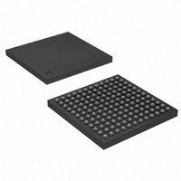
IC MCU ARM9 64K SRAM 144LFBGA
Manufacturer
Atmel
Series
AT91SAMr
Datasheet
1.AT91SAM9R64-CU.pdf
(903 pages)
Specifications of AT91SAM9R64-CU-999
Core Processor
ARM9
Core Size
16/32-Bit
Speed
240MHz
Connectivity
EBI/EMI, I²C, MMC, SPI, SSC, UART/USART, USB
Peripherals
AC'97, POR, PWM, WDT
Number Of I /o
49
Program Memory Size
32KB (32K x 8)
Program Memory Type
ROM
Ram Size
72K x 8
Voltage - Supply (vcc/vdd)
1.08 V ~ 1.32 V
Data Converters
A/D 3x10b
Oscillator Type
Internal
Operating Temperature
-40°C ~ 85°C
Package / Case
144-LFBGA
Processor Series
AT91SAMx
Core
ARM926EJ-S
Data Bus Width
32 bit
Data Ram Size
64 KB
Interface Type
SPI, TWI, UART
Maximum Clock Frequency
240 MHz
Number Of Programmable I/os
118
Operating Supply Voltage
1.65 V to 3.6 V
Maximum Operating Temperature
+ 85 C
Mounting Style
SMD/SMT
3rd Party Development Tools
JTRACE-ARM-2M, MDK-ARM, RL-ARM, ULINK2
Development Tools By Supplier
AT91SAM-ICE, AT91-ISP, AT91SAM9RL-EK
Minimum Operating Temperature
- 40 C
For Use With
AT91SAM-ICE - EMULATOR FOR AT91 ARM7/ARM9
Lead Free Status / RoHS Status
Lead free / RoHS Compliant
Eeprom Size
-
Lead Free Status / Rohs Status
Details
Available stocks
Company
Part Number
Manufacturer
Quantity
Price


6289C–ATARM–28-May-09
13 AT91SAM9R64/RL64 Debug and Test .................................................. 67
14 AT91SAM9R64/RL64 Boot Program ..................................................... 73
15 Reset Controller (RSTC) ........................................................................ 85
16 Real-time Timer (RTT) ............................................................................ 99
17 Periodic Interval Timer (PIT) ............................................................... 105
12.5 Memory Management Unit (MMU) ......................................................................61
12.6 Caches and Write Buffer .....................................................................................62
12.7 Tightly-Coupled Memory Interface ......................................................................64
12.8 Bus Interface Unit ................................................................................................65
13.1 Description ..........................................................................................................67
13.2 Block Diagram .....................................................................................................68
13.3 Application Examples ..........................................................................................69
13.4 Debug and Test Pin Description ..........................................................................70
13.5 Functional Description .........................................................................................70
14.1 Description ..........................................................................................................73
14.2 Flow Diagram ......................................................................................................73
14.3 Device Initialization ..............................................................................................74
14.4 DataFlash Boot ....................................................................................................75
14.5 SD Card Boot ......................................................................................................78
14.6 NAND Flash Boot ................................................................................................78
14.7 SAM-BA Boot ......................................................................................................79
14.8 Hardware and Software Constraints ...................................................................82
15.1 Description ..........................................................................................................85
15.2 Block Diagram .....................................................................................................85
15.3 Functional Description .........................................................................................86
15.4 Reset Controller (RSTC) User Interface ..............................................................95
16.1 Overview .............................................................................................................99
16.2 Block Diagram .....................................................................................................99
16.3 Functional Description .........................................................................................99
16.4 Real-time Timer (RTT) User Interface ...............................................................101
17.1 Overview ...........................................................................................................105
17.2 Block Diagram ...................................................................................................105
17.3 Functional Description .......................................................................................106
17.4 Periodic Interval Timer (PIT) User Interface ......................................................108
AT91SAM9R64/RL64 Preliminary
3
Related parts for AT91SAM9R64-CU-999
Image
Part Number
Description
Manufacturer
Datasheet
Request
R

Part Number:
Description:
MCU ARM9 64K SRAM 144-LFBGA
Manufacturer:
Atmel
Datasheet:

Part Number:
Description:
MCU, MPU & DSP Development Tools KICKSTART KIT FOR AT91SAM9 PLUS
Manufacturer:
IAR Systems

Part Number:
Description:
DEV KIT FOR AVR/AVR32
Manufacturer:
Atmel
Datasheet:

Part Number:
Description:
INTERVAL AND WIPE/WASH WIPER CONTROL IC WITH DELAY
Manufacturer:
ATMEL Corporation
Datasheet:
Part Number:
Description:
Low-Voltage Voice-Switched IC for Hands-Free Operation
Manufacturer:
ATMEL Corporation
Datasheet:
Part Number:
Description:
MONOLITHIC INTEGRATED FEATUREPHONE CIRCUIT
Manufacturer:
ATMEL Corporation
Datasheet:
Part Number:
Description:
AM-FM Receiver IC U4255BM-M
Manufacturer:
ATMEL Corporation
Datasheet:
Part Number:
Description:
Monolithic Integrated Feature Phone Circuit
Manufacturer:
ATMEL Corporation
Datasheet:
Part Number:
Description:
Multistandard Video-IF and Quasi Parallel Sound Processing
Manufacturer:
ATMEL Corporation
Datasheet:
Part Number:
Description:
High-performance EE PLD
Manufacturer:
ATMEL Corporation
Datasheet:
Part Number:
Description:
8-bit Flash Microcontroller
Manufacturer:
ATMEL Corporation
Datasheet: