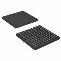
AT91SAM9R64-CU-999 Atmel, AT91SAM9R64-CU-999 Datasheet - Page 75

AT91SAM9R64-CU-999
Manufacturer Part Number
AT91SAM9R64-CU-999
Description
IC MCU ARM9 64K SRAM 144LFBGA
Manufacturer
Atmel
Series
AT91SAMr
Datasheet
1.AT91SAM9R64-CU.pdf
(903 pages)
Specifications of AT91SAM9R64-CU-999
Core Processor
ARM9
Core Size
16/32-Bit
Speed
240MHz
Connectivity
EBI/EMI, I²C, MMC, SPI, SSC, UART/USART, USB
Peripherals
AC'97, POR, PWM, WDT
Number Of I /o
49
Program Memory Size
32KB (32K x 8)
Program Memory Type
ROM
Ram Size
72K x 8
Voltage - Supply (vcc/vdd)
1.08 V ~ 1.32 V
Data Converters
A/D 3x10b
Oscillator Type
Internal
Operating Temperature
-40°C ~ 85°C
Package / Case
144-LFBGA
Processor Series
AT91SAMx
Core
ARM926EJ-S
Data Bus Width
32 bit
Data Ram Size
64 KB
Interface Type
SPI, TWI, UART
Maximum Clock Frequency
240 MHz
Number Of Programmable I/os
118
Operating Supply Voltage
1.65 V to 3.6 V
Maximum Operating Temperature
+ 85 C
Mounting Style
SMD/SMT
3rd Party Development Tools
JTRACE-ARM-2M, MDK-ARM, RL-ARM, ULINK2
Development Tools By Supplier
AT91SAM-ICE, AT91-ISP, AT91SAM9RL-EK
Minimum Operating Temperature
- 40 C
For Use With
AT91SAM-ICE - EMULATOR FOR AT91 ARM7/ARM9
Lead Free Status / RoHS Status
Lead free / RoHS Compliant
Eeprom Size
-
Lead Free Status / Rohs Status
Details
Available stocks
Company
Part Number
Manufacturer
Quantity
Price
- Current page: 75 of 903
- Download datasheet (13Mb)
Figure 14-2. Remap Action after Download Completion
14.4
After reset, the code in internal ROM is mapped at both addresses 0x0000_0000 and 0x0040_0000:
14.4.1
6289C–ATARM–28-May-09
400000
400004
400008
40000c
400010
400014
400018
DataFlash Boot
Valid Image Detection
ea000006
eafffffe
ea00002f
eafffffe
eafffffe
eafffffe
eafffffe
B
B
B
B
B
B
B
The DataFlash Boot program searches for a valid application in the SPI DataFlash memory. If a
valid application is found, this application is loaded into internal SRAM and executed by branch-
ing at address 0x0000_0000 after remap. This application may be the application code or a
second-level bootloader.
All the calls to functions are PC relative and do not use absolute addresses.
The DataFlash Boot software looks for a valid application by analyzing the first 28 bytes corre-
sponding to the ARM exception vectors. These bytes must implement ARM instructions for
either branch or load PC with PC relative addressing.
The sixth vector, at offset 0x14, contains the size of the image to download. The user must
replace this vector with his own vector (see
0x0000_0000
0x0030_0000
9. Jump to SD Card Boot sequence. If SD Card Boot succeeds, perform a remap and
10. Jump to NAND Flash Boot sequence. If NAND Flash Boot succeeds, perform a remap
11. Jump to DataFlash Boot sequence through NPCS0. If DataFlash Boot succeeds, per-
12. Activation of the Instruction Cache
13. Jump to SAM-BA Boot sequence
14. Disable the WatchDog
15. Initialization of the USB Device Port
jump to 0x0.
and jump to 0x0.
form a remap and jump to 0x0.
0x20
0x04
_main
0x0c
0x10
0x14
0x18
Internal
Internal
SRAM
ROM
REMAP
00ea000006B0x20
04eafffffeB0x04
08ea00002fB_main
0ceafffffeB0x0c
10eafffffeB0x10
14eafffffeB0x14
18eafffffeB0x18
AT91SAM9R64/RL64 Preliminary
“Structure of ARM Vector 6” on page
Internal
Internal
SRAM
ROM
0x0000_0000
0x0010_0000
76).
75
Related parts for AT91SAM9R64-CU-999
Image
Part Number
Description
Manufacturer
Datasheet
Request
R

Part Number:
Description:
MCU ARM9 64K SRAM 144-LFBGA
Manufacturer:
Atmel
Datasheet:

Part Number:
Description:
MCU, MPU & DSP Development Tools KICKSTART KIT FOR AT91SAM9 PLUS
Manufacturer:
IAR Systems

Part Number:
Description:
DEV KIT FOR AVR/AVR32
Manufacturer:
Atmel
Datasheet:

Part Number:
Description:
INTERVAL AND WIPE/WASH WIPER CONTROL IC WITH DELAY
Manufacturer:
ATMEL Corporation
Datasheet:

Part Number:
Description:
Low-Voltage Voice-Switched IC for Hands-Free Operation
Manufacturer:
ATMEL Corporation
Datasheet:

Part Number:
Description:
MONOLITHIC INTEGRATED FEATUREPHONE CIRCUIT
Manufacturer:
ATMEL Corporation
Datasheet:

Part Number:
Description:
AM-FM Receiver IC U4255BM-M
Manufacturer:
ATMEL Corporation
Datasheet:

Part Number:
Description:
Monolithic Integrated Feature Phone Circuit
Manufacturer:
ATMEL Corporation
Datasheet:

Part Number:
Description:
Multistandard Video-IF and Quasi Parallel Sound Processing
Manufacturer:
ATMEL Corporation
Datasheet:

Part Number:
Description:
High-performance EE PLD
Manufacturer:
ATMEL Corporation
Datasheet:

Part Number:
Description:
8-bit Flash Microcontroller
Manufacturer:
ATMEL Corporation
Datasheet:


