AT91SAM9R64-CU-999 Atmel, AT91SAM9R64-CU-999 Datasheet - Page 396
AT91SAM9R64-CU-999
Manufacturer Part Number
AT91SAM9R64-CU-999
Description
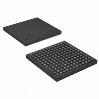
IC MCU ARM9 64K SRAM 144LFBGA
Manufacturer
Atmel
Series
AT91SAMr
Datasheet
1.AT91SAM9R64-CU.pdf
(903 pages)
Specifications of AT91SAM9R64-CU-999
Core Processor
ARM9
Core Size
16/32-Bit
Speed
240MHz
Connectivity
EBI/EMI, I²C, MMC, SPI, SSC, UART/USART, USB
Peripherals
AC'97, POR, PWM, WDT
Number Of I /o
49
Program Memory Size
32KB (32K x 8)
Program Memory Type
ROM
Ram Size
72K x 8
Voltage - Supply (vcc/vdd)
1.08 V ~ 1.32 V
Data Converters
A/D 3x10b
Oscillator Type
Internal
Operating Temperature
-40°C ~ 85°C
Package / Case
144-LFBGA
Processor Series
AT91SAMx
Core
ARM926EJ-S
Data Bus Width
32 bit
Data Ram Size
64 KB
Interface Type
SPI, TWI, UART
Maximum Clock Frequency
240 MHz
Number Of Programmable I/os
118
Operating Supply Voltage
1.65 V to 3.6 V
Maximum Operating Temperature
+ 85 C
Mounting Style
SMD/SMT
3rd Party Development Tools
JTRACE-ARM-2M, MDK-ARM, RL-ARM, ULINK2
Development Tools By Supplier
AT91SAM-ICE, AT91-ISP, AT91SAM9RL-EK
Minimum Operating Temperature
- 40 C
For Use With
AT91SAM-ICE - EMULATOR FOR AT91 ARM7/ARM9
Lead Free Status / RoHS Status
Lead free / RoHS Compliant
Eeprom Size
-
Lead Free Status / Rohs Status
Details
Available stocks
Company
Part Number
Manufacturer
Quantity
Price


32.7.9
Name:
Access Type:
• CPOL: Clock Polarity
0 = The inactive state value of SPCK is logic level zero.
1 = The inactive state value of SPCK is logic level one.
CPOL is used to determine the inactive state value of the serial clock (SPCK). It is used with NCPHA to produce the
required clock/data relationship between master and slave devices.
• NCPHA: Clock Phase
0 = Data is changed on the leading edge of SPCK and captured on the following edge of SPCK.
1 = Data is captured on the leading edge of SPCK and changed on the following edge of SPCK.
NCPHA determines which edge of SPCK causes data to change and which edge causes data to be captured. NCPHA is
used with CPOL to produce the required clock/data relationship between master and slave devices.
• CSAAT: Chip Select Active After Transfer
0 = The Peripheral Chip Select Line rises as soon as the last transfer is achieved.
1 = The Peripheral Chip Select does not rise after the last transfer is achieved. It remains active until a new transfer is
requested on a different chip select.
• BITS: Bits Per Transfer
The BITS field determines the number of data bits transferred. Reserved values should not be used.
6289C–ATARM–28-May-09
31
23
15
7
SPI Chip Select Register
30
22
14
SPI_CSR0... SPI_CSR3
Read/Write
6
BITS
0000
0001
0010
0011
0100
0101
0110
0111
1000
BITS
29
21
13
5
28
20
12
4
DLYBCT
DLYBS
SCBR
AT91SAM9R64/RL64 Preliminary
CSAAT
27
19
11
3
Bits Per Transfer
26
18
10
–
2
10
11
12
13
14
15
16
8
9
NCPHA
25
17
9
1
CPOL
24
16
8
0
396
Related parts for AT91SAM9R64-CU-999
Image
Part Number
Description
Manufacturer
Datasheet
Request
R

Part Number:
Description:
MCU ARM9 64K SRAM 144-LFBGA
Manufacturer:
Atmel
Datasheet:

Part Number:
Description:
MCU, MPU & DSP Development Tools KICKSTART KIT FOR AT91SAM9 PLUS
Manufacturer:
IAR Systems

Part Number:
Description:
DEV KIT FOR AVR/AVR32
Manufacturer:
Atmel
Datasheet:

Part Number:
Description:
INTERVAL AND WIPE/WASH WIPER CONTROL IC WITH DELAY
Manufacturer:
ATMEL Corporation
Datasheet:
Part Number:
Description:
Low-Voltage Voice-Switched IC for Hands-Free Operation
Manufacturer:
ATMEL Corporation
Datasheet:
Part Number:
Description:
MONOLITHIC INTEGRATED FEATUREPHONE CIRCUIT
Manufacturer:
ATMEL Corporation
Datasheet:
Part Number:
Description:
AM-FM Receiver IC U4255BM-M
Manufacturer:
ATMEL Corporation
Datasheet:
Part Number:
Description:
Monolithic Integrated Feature Phone Circuit
Manufacturer:
ATMEL Corporation
Datasheet:
Part Number:
Description:
Multistandard Video-IF and Quasi Parallel Sound Processing
Manufacturer:
ATMEL Corporation
Datasheet:
Part Number:
Description:
High-performance EE PLD
Manufacturer:
ATMEL Corporation
Datasheet:
Part Number:
Description:
8-bit Flash Microcontroller
Manufacturer:
ATMEL Corporation
Datasheet: