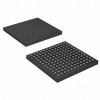
AT91SAM9R64-CU-999 Atmel, AT91SAM9R64-CU-999 Datasheet - Page 259

AT91SAM9R64-CU-999
Manufacturer Part Number
AT91SAM9R64-CU-999
Description
IC MCU ARM9 64K SRAM 144LFBGA
Manufacturer
Atmel
Series
AT91SAMr
Datasheet
1.AT91SAM9R64-CU.pdf
(903 pages)
Specifications of AT91SAM9R64-CU-999
Core Processor
ARM9
Core Size
16/32-Bit
Speed
240MHz
Connectivity
EBI/EMI, I²C, MMC, SPI, SSC, UART/USART, USB
Peripherals
AC'97, POR, PWM, WDT
Number Of I /o
49
Program Memory Size
32KB (32K x 8)
Program Memory Type
ROM
Ram Size
72K x 8
Voltage - Supply (vcc/vdd)
1.08 V ~ 1.32 V
Data Converters
A/D 3x10b
Oscillator Type
Internal
Operating Temperature
-40°C ~ 85°C
Package / Case
144-LFBGA
Processor Series
AT91SAMx
Core
ARM926EJ-S
Data Bus Width
32 bit
Data Ram Size
64 KB
Interface Type
SPI, TWI, UART
Maximum Clock Frequency
240 MHz
Number Of Programmable I/os
118
Operating Supply Voltage
1.65 V to 3.6 V
Maximum Operating Temperature
+ 85 C
Mounting Style
SMD/SMT
3rd Party Development Tools
JTRACE-ARM-2M, MDK-ARM, RL-ARM, ULINK2
Development Tools By Supplier
AT91SAM-ICE, AT91-ISP, AT91SAM9RL-EK
Minimum Operating Temperature
- 40 C
For Use With
AT91SAM-ICE - EMULATOR FOR AT91 ARM7/ARM9
Lead Free Status / RoHS Status
Lead free / RoHS Compliant
Eeprom Size
-
Lead Free Status / Rohs Status
Details
Available stocks
Company
Part Number
Manufacturer
Quantity
Price
- Current page: 259 of 903
- Download datasheet (13Mb)
26.5.4
26.6
26.6.1
6289C–ATARM–28-May-09
Divider and PLL Block
Main Oscillator Bypass
PLL Filter
When enabling the main oscillator, the user must initiate the main oscillator counter with a value
corresponding to the startup time of the oscillator. This startup time depends on the crystal fre-
quency connected to the main oscillator.
When the MOSCEN bit and the OSCOUNT are written in CKGR_MOR to enable the main oscil-
lator, the MOSCS bit in PMC_SR (Status Register) is cleared and the counter starts counting
down on the slow clock divided by 8 from the OSCOUNT value. Since the OSCOUNT value is
coded with 8 bits, the maximum startup time is about 62 ms.
When the counter reaches 0, the MOSCS bit is set, indicating that the main clock is valid. Set-
ting the MOSCS bit in PMC_IMR can trigger an interrupt to the processor.
The user can input a clock on the device instead of connecting a crystal. In this case, the user
has to provide the external clock signal on the XIN pin. The input characteristics of the XIN pin
under these conditions are given in the product electrical characteristics section. The program-
mer has to be sure to set the OSCBYPASS bit to 1 and the MOSCEN bit to 0 in the Main OSC
register (CKGR_MOR) for the external clock to operate properly.
The PLL embeds an input divider to increase the accuracy of the resulting clock signals. How-
ever, the user must respect the PLL minimum input frequency when programming the divider.
Figure 26-5
Figure 26-5. Divider and PLL Block Diagram
The PLL requires connection to an external second-order filter through the PLLRC pin.
26-6
shows a schematic of these filters.
shows the block diagram of the divider and PLL block.
MAINCK
SLCK
AT91SAM9R64/RL64 Preliminary
Divider
DIV
PLLCOUNT
Counter
PLLRC
PLL
MUL
PLL
OUT
LOCK
PLLCK
Figure
259
Related parts for AT91SAM9R64-CU-999
Image
Part Number
Description
Manufacturer
Datasheet
Request
R

Part Number:
Description:
MCU ARM9 64K SRAM 144-LFBGA
Manufacturer:
Atmel
Datasheet:

Part Number:
Description:
MCU, MPU & DSP Development Tools KICKSTART KIT FOR AT91SAM9 PLUS
Manufacturer:
IAR Systems

Part Number:
Description:
DEV KIT FOR AVR/AVR32
Manufacturer:
Atmel
Datasheet:

Part Number:
Description:
INTERVAL AND WIPE/WASH WIPER CONTROL IC WITH DELAY
Manufacturer:
ATMEL Corporation
Datasheet:

Part Number:
Description:
Low-Voltage Voice-Switched IC for Hands-Free Operation
Manufacturer:
ATMEL Corporation
Datasheet:

Part Number:
Description:
MONOLITHIC INTEGRATED FEATUREPHONE CIRCUIT
Manufacturer:
ATMEL Corporation
Datasheet:

Part Number:
Description:
AM-FM Receiver IC U4255BM-M
Manufacturer:
ATMEL Corporation
Datasheet:

Part Number:
Description:
Monolithic Integrated Feature Phone Circuit
Manufacturer:
ATMEL Corporation
Datasheet:

Part Number:
Description:
Multistandard Video-IF and Quasi Parallel Sound Processing
Manufacturer:
ATMEL Corporation
Datasheet:

Part Number:
Description:
High-performance EE PLD
Manufacturer:
ATMEL Corporation
Datasheet:

Part Number:
Description:
8-bit Flash Microcontroller
Manufacturer:
ATMEL Corporation
Datasheet:


