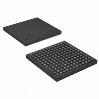
AT91SAM9R64-CU-999 Atmel, AT91SAM9R64-CU-999 Datasheet - Page 661

AT91SAM9R64-CU-999
Manufacturer Part Number
AT91SAM9R64-CU-999
Description
IC MCU ARM9 64K SRAM 144LFBGA
Manufacturer
Atmel
Series
AT91SAMr
Datasheet
1.AT91SAM9R64-CU.pdf
(903 pages)
Specifications of AT91SAM9R64-CU-999
Core Processor
ARM9
Core Size
16/32-Bit
Speed
240MHz
Connectivity
EBI/EMI, I²C, MMC, SPI, SSC, UART/USART, USB
Peripherals
AC'97, POR, PWM, WDT
Number Of I /o
49
Program Memory Size
32KB (32K x 8)
Program Memory Type
ROM
Ram Size
72K x 8
Voltage - Supply (vcc/vdd)
1.08 V ~ 1.32 V
Data Converters
A/D 3x10b
Oscillator Type
Internal
Operating Temperature
-40°C ~ 85°C
Package / Case
144-LFBGA
Processor Series
AT91SAMx
Core
ARM926EJ-S
Data Bus Width
32 bit
Data Ram Size
64 KB
Interface Type
SPI, TWI, UART
Maximum Clock Frequency
240 MHz
Number Of Programmable I/os
118
Operating Supply Voltage
1.65 V to 3.6 V
Maximum Operating Temperature
+ 85 C
Mounting Style
SMD/SMT
3rd Party Development Tools
JTRACE-ARM-2M, MDK-ARM, RL-ARM, ULINK2
Development Tools By Supplier
AT91SAM-ICE, AT91-ISP, AT91SAM9RL-EK
Minimum Operating Temperature
- 40 C
For Use With
AT91SAM-ICE - EMULATOR FOR AT91 ARM7/ARM9
Lead Free Status / RoHS Status
Lead free / RoHS Compliant
Eeprom Size
-
Lead Free Status / Rohs Status
Details
Available stocks
Company
Part Number
Manufacturer
Quantity
Price
- Current page: 661 of 903
- Download datasheet (13Mb)
39.5.2.8
6289C–ATARM–28-May-09
Timegen
For a more detailed description of the LCD Interface, see
The time generator block generates the control signals LCDDOTCK, LCDHSYNC, LCDVSYNC,
LCDDEN, used by the LCD module. This block is programmable in order to support different
types of LCD modules and obtain the output clock signals, which are derived from the LCDC
Core clock.
The LCDDOTCK signal is used to clock the data into the LCD drivers' shift register. The data is
sent through LCDD[23:0] synchronized by default with LCDDOTCK falling edge (rising edge can
be selected). The CLKVAL field of LCDCON1 register controls the rate of this signal. The divisor
can also be bypassed with the BYPASS bit in the LCDCON1 register. In this case, the rate of
LCDDOTCK is equal to the frequency of the LCDC Core clock. The minimum period of the LCD-
DOTCK signal depends on the configuration. This information can be found in
The LCDDOTCK signal has two different timings that are selected with the CLKMOD field of the
LCDCON2 register:
Table 39-11. Minimum LCDDOTCK Period in LCDC Core Clock Cycles
The LCDDEN signal indicates valid data in the LCD Interface.
After each horizontal line of data has been shifted into the LCD, the LCDHSYNC is asserted to
cause the line to be displayed on the panel.
The following timing parameters can be configured:
DISTYPE
TFT
STN Mono
STN Mono
STN Mono
STN Mono
STN Color
STN Color
STN Color
STN Color
• Always Active (used with TFT LCD Modules)
• Active only when data is available (used with STN LCD Modules)
f
LCDDOTCK
SCAN
Single
Single
Dual
Dual
Single
Single
Dual
Dual
=
-------------------------------- -
2
Configuration
f
LCDC_clock
×
CLKVAL
AT91SAM9R64/RL64 Preliminary
IFWIDTH
4
8
8
16
4
8
8
16
“LCD Interface” on page
LCDDOTCK Period
1
4
8
8
16
2
2
4
6
Table
666.
39-11.
661
Related parts for AT91SAM9R64-CU-999
Image
Part Number
Description
Manufacturer
Datasheet
Request
R

Part Number:
Description:
MCU ARM9 64K SRAM 144-LFBGA
Manufacturer:
Atmel
Datasheet:

Part Number:
Description:
MCU, MPU & DSP Development Tools KICKSTART KIT FOR AT91SAM9 PLUS
Manufacturer:
IAR Systems

Part Number:
Description:
DEV KIT FOR AVR/AVR32
Manufacturer:
Atmel
Datasheet:

Part Number:
Description:
INTERVAL AND WIPE/WASH WIPER CONTROL IC WITH DELAY
Manufacturer:
ATMEL Corporation
Datasheet:

Part Number:
Description:
Low-Voltage Voice-Switched IC for Hands-Free Operation
Manufacturer:
ATMEL Corporation
Datasheet:

Part Number:
Description:
MONOLITHIC INTEGRATED FEATUREPHONE CIRCUIT
Manufacturer:
ATMEL Corporation
Datasheet:

Part Number:
Description:
AM-FM Receiver IC U4255BM-M
Manufacturer:
ATMEL Corporation
Datasheet:

Part Number:
Description:
Monolithic Integrated Feature Phone Circuit
Manufacturer:
ATMEL Corporation
Datasheet:

Part Number:
Description:
Multistandard Video-IF and Quasi Parallel Sound Processing
Manufacturer:
ATMEL Corporation
Datasheet:

Part Number:
Description:
High-performance EE PLD
Manufacturer:
ATMEL Corporation
Datasheet:

Part Number:
Description:
8-bit Flash Microcontroller
Manufacturer:
ATMEL Corporation
Datasheet:


