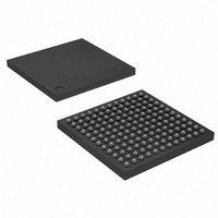
AT91SAM9R64-CU-999 Atmel, AT91SAM9R64-CU-999 Datasheet - Page 19

AT91SAM9R64-CU-999
Manufacturer Part Number
AT91SAM9R64-CU-999
Description
IC MCU ARM9 64K SRAM 144LFBGA
Manufacturer
Atmel
Series
AT91SAMr
Datasheet
1.AT91SAM9R64-CU.pdf
(903 pages)
Specifications of AT91SAM9R64-CU-999
Core Processor
ARM9
Core Size
16/32-Bit
Speed
240MHz
Connectivity
EBI/EMI, I²C, MMC, SPI, SSC, UART/USART, USB
Peripherals
AC'97, POR, PWM, WDT
Number Of I /o
49
Program Memory Size
32KB (32K x 8)
Program Memory Type
ROM
Ram Size
72K x 8
Voltage - Supply (vcc/vdd)
1.08 V ~ 1.32 V
Data Converters
A/D 3x10b
Oscillator Type
Internal
Operating Temperature
-40°C ~ 85°C
Package / Case
144-LFBGA
Processor Series
AT91SAMx
Core
ARM926EJ-S
Data Bus Width
32 bit
Data Ram Size
64 KB
Interface Type
SPI, TWI, UART
Maximum Clock Frequency
240 MHz
Number Of Programmable I/os
118
Operating Supply Voltage
1.65 V to 3.6 V
Maximum Operating Temperature
+ 85 C
Mounting Style
SMD/SMT
3rd Party Development Tools
JTRACE-ARM-2M, MDK-ARM, RL-ARM, ULINK2
Development Tools By Supplier
AT91SAM-ICE, AT91-ISP, AT91SAM9RL-EK
Minimum Operating Temperature
- 40 C
For Use With
AT91SAM-ICE - EMULATOR FOR AT91 ARM7/ARM9
Lead Free Status / RoHS Status
Lead free / RoHS Compliant
Eeprom Size
-
Lead Free Status / Rohs Status
Details
Available stocks
Company
Part Number
Manufacturer
Quantity
Price
- Current page: 19 of 903
- Download datasheet (13Mb)
7.2
6289C–ATARM–28-May-09
Matrix Masters
•
•
•
•
•
•
The Bus Matrix of the AT91SAM9R64/RL64 product manages 6 masters, which means that
each master can perform an access concurrently with others, to an available slave.
Each master has its own decoder, which is defined specifically for each master. In order to sim-
plify the addressing, all the masters have the same decodings.
Table 7-1.
Master 0
Master 1
Master 2
–
–
DSP Instruction Extensions
5-Stage Pipeline Architecture:
–
–
–
–
–
4-Kbyte Data Cache, 4-Kbyte Instruction Cache
–
–
–
–
Write Buffer
–
–
–
Standard ARM v4 and v5 Memory Management Unit (MMU)
–
–
–
Bus Interface Unit (BIU)
–
–
–
–
ARM High-performance 32-bit Instruction Set
Thumb High Code Density 16-bit Instruction Set
Instruction Fetch (F)
Instruction Decode (D)
Execute (E)
Data Memory (M)
Register Write (W)
Virtually-addressed 4-way Associative Cache
Eight words per line
Write-through and Write-back Operation
Pseudo-random or Round-robin Replacement
Main Write Buffer with 16-word Data Buffer and 4-address Buffer
DCache Write-back Buffer with 8-word Entries and a Single Address Entry
Software Control Drain
Access Permission for Sections
Access Permission for large pages and small pages can be specified separately for
each quarter of the page
16 embedded domains
Arbitrates and Schedules AHB Requests
Separate Masters for both instruction and data access providing complete Matrix
system flexibility
Separate Address and Data Buses for both the 32-bit instruction interface and the
32-bit data interface
On Address and Data Buses, data can be 8-bit (Bytes), 16-bit (Half-words) or 32-bit
(Words)
List of Bus Matrix Masters
DMA Controller
USB Device High Speed DMA
LCD Controller DMA
AT91SAM9R64/RL64 Preliminary
19
Related parts for AT91SAM9R64-CU-999
Image
Part Number
Description
Manufacturer
Datasheet
Request
R

Part Number:
Description:
MCU ARM9 64K SRAM 144-LFBGA
Manufacturer:
Atmel
Datasheet:

Part Number:
Description:
MCU, MPU & DSP Development Tools KICKSTART KIT FOR AT91SAM9 PLUS
Manufacturer:
IAR Systems

Part Number:
Description:
DEV KIT FOR AVR/AVR32
Manufacturer:
Atmel
Datasheet:

Part Number:
Description:
INTERVAL AND WIPE/WASH WIPER CONTROL IC WITH DELAY
Manufacturer:
ATMEL Corporation
Datasheet:

Part Number:
Description:
Low-Voltage Voice-Switched IC for Hands-Free Operation
Manufacturer:
ATMEL Corporation
Datasheet:

Part Number:
Description:
MONOLITHIC INTEGRATED FEATUREPHONE CIRCUIT
Manufacturer:
ATMEL Corporation
Datasheet:

Part Number:
Description:
AM-FM Receiver IC U4255BM-M
Manufacturer:
ATMEL Corporation
Datasheet:

Part Number:
Description:
Monolithic Integrated Feature Phone Circuit
Manufacturer:
ATMEL Corporation
Datasheet:

Part Number:
Description:
Multistandard Video-IF and Quasi Parallel Sound Processing
Manufacturer:
ATMEL Corporation
Datasheet:

Part Number:
Description:
High-performance EE PLD
Manufacturer:
ATMEL Corporation
Datasheet:

Part Number:
Description:
8-bit Flash Microcontroller
Manufacturer:
ATMEL Corporation
Datasheet:


