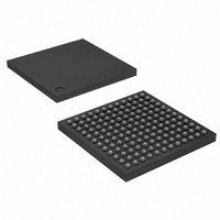
AT91SAM9R64-CU-999 Atmel, AT91SAM9R64-CU-999 Datasheet - Page 740

AT91SAM9R64-CU-999
Manufacturer Part Number
AT91SAM9R64-CU-999
Description
IC MCU ARM9 64K SRAM 144LFBGA
Manufacturer
Atmel
Series
AT91SAMr
Datasheet
1.AT91SAM9R64-CU.pdf
(903 pages)
Specifications of AT91SAM9R64-CU-999
Core Processor
ARM9
Core Size
16/32-Bit
Speed
240MHz
Connectivity
EBI/EMI, I²C, MMC, SPI, SSC, UART/USART, USB
Peripherals
AC'97, POR, PWM, WDT
Number Of I /o
49
Program Memory Size
32KB (32K x 8)
Program Memory Type
ROM
Ram Size
72K x 8
Voltage - Supply (vcc/vdd)
1.08 V ~ 1.32 V
Data Converters
A/D 3x10b
Oscillator Type
Internal
Operating Temperature
-40°C ~ 85°C
Package / Case
144-LFBGA
Processor Series
AT91SAMx
Core
ARM926EJ-S
Data Bus Width
32 bit
Data Ram Size
64 KB
Interface Type
SPI, TWI, UART
Maximum Clock Frequency
240 MHz
Number Of Programmable I/os
118
Operating Supply Voltage
1.65 V to 3.6 V
Maximum Operating Temperature
+ 85 C
Mounting Style
SMD/SMT
3rd Party Development Tools
JTRACE-ARM-2M, MDK-ARM, RL-ARM, ULINK2
Development Tools By Supplier
AT91SAM-ICE, AT91-ISP, AT91SAM9RL-EK
Minimum Operating Temperature
- 40 C
For Use With
AT91SAM-ICE - EMULATOR FOR AT91 ARM7/ARM9
Lead Free Status / RoHS Status
Lead free / RoHS Compliant
Eeprom Size
-
Lead Free Status / Rohs Status
Details
Available stocks
Company
Part Number
Manufacturer
Quantity
Price
- Current page: 740 of 903
- Download datasheet (13Mb)
41.4.6
Figure 41-5. Example of DMA Chained List:
740
(Current Transfer Descriptor)
UDPHS Next Descriptor
DMA Channel Address
DMA Channel Control
UDPHS Registers
Memory Area
Data Buff 1
Data Buff 2
Data Buff 3
AT91SAM9R64/RL64 Preliminary
Transfer With DMA
USB packets of any length may be transferred when required by the UDPHS Device. These
transfers always feature sequential addressing.
Packet data AHB bursts may be locked on a DMA buffer basis for drastic overall AHB bus band-
width performance boost with paged memories. These clock-cycle consuming memory row (or
bank) changes will then likely not occur, or occur only once instead of dozens times, during a
single big USB packet DMA transfer in case another AHB master addresses the memory. This
means up to 128-word single-cycle unbroken AHB bursts for Bulk endpoints and 256-word sin-
gle-cycle unbroken bursts for isochronous endpoints. This maximum burst length is then
c o n t r o l l e d b y t h e l o w e s t p r o g r a m m e d U S B e n d p o i n t s i z e ( E P T _ S I Z E b i t i n t h e
U D P H S _ E P T C F G x r e g i s t e r ) a n d D M A S i z e ( B U F F _ L E N G T H b i t i n t h e
UDPHS_DMACONTROLx register).
The USB 2.0 device average throughput may be up to nearly 60 MBytes. Its internal slave aver-
age access latency decreases as burst length increases due to the 0 wait-state side effect of
unchanged endpoints. If at least 0 wait-state word burst capability is also provided by the exter-
nal DMA AHB bus slaves, each of both DMA AHB busses need less than 50% bandwidth
allocation for full USB 2.0 bandwidth usage at 30 MHz, and less than 25% at 60 MHz.
The UDPHS DMA Channel Transfer Descriptor is described in
Descriptor” on page
Note: In case of debug, be careful to address the DMA to an SRAM address even if a remap is
done.
Next Descriptor Address
DMA Channel Address
DMA Channel Control
Transfer Descriptor
798.
Next Descriptor Address
DMA Channel Address
DMA Channel Control
Transfer Descriptor
Next Descriptor Address
DMA Channel Address
“UDPHS DMA Channel Transfer
DMA Channel Control
Transfer Descriptor
6289C–ATARM–28-May-09
Null
Related parts for AT91SAM9R64-CU-999
Image
Part Number
Description
Manufacturer
Datasheet
Request
R

Part Number:
Description:
MCU ARM9 64K SRAM 144-LFBGA
Manufacturer:
Atmel
Datasheet:

Part Number:
Description:
MCU, MPU & DSP Development Tools KICKSTART KIT FOR AT91SAM9 PLUS
Manufacturer:
IAR Systems

Part Number:
Description:
DEV KIT FOR AVR/AVR32
Manufacturer:
Atmel
Datasheet:

Part Number:
Description:
INTERVAL AND WIPE/WASH WIPER CONTROL IC WITH DELAY
Manufacturer:
ATMEL Corporation
Datasheet:

Part Number:
Description:
Low-Voltage Voice-Switched IC for Hands-Free Operation
Manufacturer:
ATMEL Corporation
Datasheet:

Part Number:
Description:
MONOLITHIC INTEGRATED FEATUREPHONE CIRCUIT
Manufacturer:
ATMEL Corporation
Datasheet:

Part Number:
Description:
AM-FM Receiver IC U4255BM-M
Manufacturer:
ATMEL Corporation
Datasheet:

Part Number:
Description:
Monolithic Integrated Feature Phone Circuit
Manufacturer:
ATMEL Corporation
Datasheet:

Part Number:
Description:
Multistandard Video-IF and Quasi Parallel Sound Processing
Manufacturer:
ATMEL Corporation
Datasheet:

Part Number:
Description:
High-performance EE PLD
Manufacturer:
ATMEL Corporation
Datasheet:

Part Number:
Description:
8-bit Flash Microcontroller
Manufacturer:
ATMEL Corporation
Datasheet:


