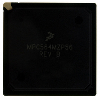
MPC564MZP56 Freescale Semiconductor, MPC564MZP56 Datasheet - Page 987

MPC564MZP56
Manufacturer Part Number
MPC564MZP56
Description
IC MCU 512K FLASH 56MHZ 388-BGA
Manufacturer
Freescale Semiconductor
Series
MPC5xxr
Specifications of MPC564MZP56
Core Processor
PowerPC
Core Size
32-Bit
Speed
56MHz
Connectivity
CAN, EBI/EMI, SCI, SPI, UART/USART
Peripherals
POR, PWM, WDT
Number Of I /o
56
Program Memory Size
512KB (512K x 8)
Program Memory Type
FLASH
Ram Size
32K x 8
Voltage - Supply (vcc/vdd)
2.5 V ~ 2.7 V
Data Converters
A/D 32x10b
Oscillator Type
External
Operating Temperature
-40°C ~ 125°C
Package / Case
388-BGA
Core
PowerPC
Processor Series
MPC5xx
Data Bus Width
32 bit
Maximum Clock Frequency
56 MHz
Data Ram Size
32 KB
On-chip Adc
Yes
Number Of Programmable I/os
56
Number Of Timers
2
Operating Supply Voltage
0 V to 5 V
Mounting Style
SMD/SMT
A/d Bit Size
10 bit
A/d Channels Available
32
Height
1.95 mm
Interface Type
CAN, JTAG, QSPI, SCI, SPI, UART
Length
27 mm
Maximum Operating Temperature
+ 125 C
Minimum Operating Temperature
- 40 C
Supply Voltage (max)
2.7 V, 5.25 V
Supply Voltage (min)
2.5 V, 4.75 V
Width
27 mm
For Use With
MPC564EVB - KIT EVAL FOR MPC561/562/563/564
Lead Free Status / RoHS Status
Contains lead / RoHS non-compliant
Eeprom Size
-
Lead Free Status / Rohs Status
No RoHS Version Available
Available stocks
Company
Part Number
Manufacturer
Quantity
Price
Company:
Part Number:
MPC564MZP56
Manufacturer:
FREESCAL
Quantity:
364
Company:
Part Number:
MPC564MZP56
Manufacturer:
Freescale Semiconductor
Quantity:
10 000
Part Number:
MPC564MZP56
Manufacturer:
FREESCALE
Quantity:
20 000
Company:
Part Number:
MPC564MZP56R2
Manufacturer:
Freescale Semiconductor
Quantity:
10 000
- Current page: 987 of 1420
- Download datasheet (11Mb)
To read control or status from memory-mapped locations the following sequence would be required.
For a block write to memory-mapped locations the following sequence would be required.
For a block read from memory-mapped locations the following sequence would be required.
Refer to
24.6.3
To write control or status data to READI tool mapped registers the following sequence would be required.
To read control or status from READI tool mapped registers the following sequence would be required
Refer to
24.6.4
Registers may be updated via the auxiliary port using the download request message with the message
containing only N (where N is less than register width) most-significant bits of the register. In such cases
the bits not transmitted will be reset to 0b0. The bits transmitted will be aligned such that the last bit
transmitted will be the most significant bit of the register. Therefore a message size that is divisible by the
input port size should be transmitted.
Freescale Semiconductor
1. The tool confirms that the device is ready. The tool transmits the download request public message
2. When device reads data it transmits upload/download information message (TCODE 19)
1. The tool confirms that the device is ready. The tool transmits the download request public message
2. The tool waits for device ready for upload/download message (TCODE 16). When it is transmitted
1. The tool confirms that the device is ready. The tool transmits the download request public message
2. The tool waits for upload/download information message (TCODE 19) from device, which
1. The tool confirms that the device is ready. The tool transmits the download request message
2. The tool waits for device ready for upload/download message (TCODE 16) before initiating next
1. The tool confirms that the device is ready. The tool transmits the upload request message (TCODE
2. When device reads data it transmits upload/download information message (TCODE 19)
(TCODE 18) which contains read attributes and target address.
containing read data. Device is now ready for next access.
(TCODE 18) which contains block write attributes, first write data, and target address.
by device, tool transmits upload/download information message (TCODE 19) containing next
write data. This step is repeated until all data is written
(TCODE 18) which contains block read attributes and target address.
contains read data. This step is repeated until all data is read.
(TCODE 18) which contains write data, and register opcode.
access.
17) which contains the target opcode.
containing read data. Device is now ready for next access.
Section 24.10, “Read/Write
Section 24.10, “Read/Write
Accessing READI Tool Mapped Registers Via the Auxiliary Port
Partial Register Updates
MPC561/MPC563 Reference Manual, Rev. 1.2
Access,” for more details on read/write access protocol.
Access,” for more details on read/write access protocol.
READI Module
24-19
Related parts for MPC564MZP56
Image
Part Number
Description
Manufacturer
Datasheet
Request
R

Part Number:
Description:
MPC5 1K0 5%
Manufacturer:
TE Connectivity
Datasheet:

Part Number:
Description:
MPC5 500R 5%
Manufacturer:
TE Connectivity
Datasheet:

Part Number:
Description:
MPC5 5K0 5%
Manufacturer:
Tyco Electronics
Datasheet:

Part Number:
Description:
MPC5 5R0 5%
Manufacturer:
Tyco Electronics
Datasheet:

Part Number:
Description:
MPC5 50K 5%
Manufacturer:
Tyco Electronics
Datasheet:

Part Number:
Description:
MPC5 1R0 5%
Manufacturer:
Tyco Electronics
Datasheet:
Part Number:
Description:
Manufacturer:
Freescale Semiconductor, Inc
Datasheet:
Part Number:
Description:
Manufacturer:
Freescale Semiconductor, Inc
Datasheet:
Part Number:
Description:
Manufacturer:
Freescale Semiconductor, Inc
Datasheet:
Part Number:
Description:
Manufacturer:
Freescale Semiconductor, Inc
Datasheet:
Part Number:
Description:
Manufacturer:
Freescale Semiconductor, Inc
Datasheet:


