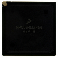
MPC564MZP56 Freescale Semiconductor, MPC564MZP56 Datasheet - Page 983

MPC564MZP56
Manufacturer Part Number
MPC564MZP56
Description
IC MCU 512K FLASH 56MHZ 388-BGA
Manufacturer
Freescale Semiconductor
Series
MPC5xxr
Specifications of MPC564MZP56
Core Processor
PowerPC
Core Size
32-Bit
Speed
56MHz
Connectivity
CAN, EBI/EMI, SCI, SPI, UART/USART
Peripherals
POR, PWM, WDT
Number Of I /o
56
Program Memory Size
512KB (512K x 8)
Program Memory Type
FLASH
Ram Size
32K x 8
Voltage - Supply (vcc/vdd)
2.5 V ~ 2.7 V
Data Converters
A/D 32x10b
Oscillator Type
External
Operating Temperature
-40°C ~ 125°C
Package / Case
388-BGA
Core
PowerPC
Processor Series
MPC5xx
Data Bus Width
32 bit
Maximum Clock Frequency
56 MHz
Data Ram Size
32 KB
On-chip Adc
Yes
Number Of Programmable I/os
56
Number Of Timers
2
Operating Supply Voltage
0 V to 5 V
Mounting Style
SMD/SMT
A/d Bit Size
10 bit
A/d Channels Available
32
Height
1.95 mm
Interface Type
CAN, JTAG, QSPI, SCI, SPI, UART
Length
27 mm
Maximum Operating Temperature
+ 125 C
Minimum Operating Temperature
- 40 C
Supply Voltage (max)
2.7 V, 5.25 V
Supply Voltage (min)
2.5 V, 4.75 V
Width
27 mm
For Use With
MPC564EVB - KIT EVAL FOR MPC561/562/563/564
Lead Free Status / RoHS Status
Contains lead / RoHS non-compliant
Eeprom Size
-
Lead Free Status / Rohs Status
No RoHS Version Available
Available stocks
Company
Part Number
Manufacturer
Quantity
Price
Company:
Part Number:
MPC564MZP56
Manufacturer:
FREESCAL
Quantity:
364
Company:
Part Number:
MPC564MZP56
Manufacturer:
Freescale Semiconductor
Quantity:
10 000
Part Number:
MPC564MZP56
Manufacturer:
FREESCALE
Quantity:
20 000
Company:
Part Number:
MPC564MZP56R2
Manufacturer:
Freescale Semiconductor
Quantity:
10 000
- Current page: 983 of 1420
- Download datasheet (11Mb)
24.6.1.8
The UDI register, a 34-bit register, is used to store the data to be written for block write access, and the
data read for read (single and block) accesses.
Freescale Semiconductor
RCPU
27:28
29:60
61:62
64:79
Bits
63
Nexus
52:51
50:19
18:17
Upload/Download Information Register (UDI)
Bits
15:0
16
Table 24-11. RWA Read/Write Access Bit Descriptions (continued)
Name
MAP
CNT
PRV
WD
SZ
The word size (SZ) field can be configured to allow 32-bit, 16-bit, or 8-bit read/write
accesses. If the field is configured to one of the reserved states, its action reverts to
that of the default state.
00 32-bit
01 16-bit
10 8-bit
11 Reserved
Write data (WD) bits contain the data to be written. For a read access, the data stored
is a don’t care.
The Privilege Attribute Field can be configured to select different read/write access
attributes.
00 User Data
01 User Instruction
10 Supervisor Data
11 Supervisor Instruction
The Map Select Field can be configured to allow access to multiple memory maps.
The primary processor memory map (MAP equal to 0b0) is designated as the default.
The secondary memory map (MAP equal to 0b1) can be set to select the MPC500
special purpose registers.
0 Primary memory map
1 Secondary memory map (PPC Special Purpose Registers)
The Access Count Field can be configured to indicate the number of accesses of word
size (defined in SZ field). The CNT value is used to increment the specified address
in the RWAD field for block read/write accesses.
For a single read/write access, the CNT value should equal to 0x0000. A 64-Kbyte
block read/write access can be performed by configuring the CNT bits as 0xFFFF. If
a user wants to terminate a block read or write access which has not completed, the
CNT bits should be reset.
MPC561/MPC563 Reference Manual, Rev. 1.2
Table 24-12
gives a description of the register bits.
Description
READI Module
24-15
Related parts for MPC564MZP56
Image
Part Number
Description
Manufacturer
Datasheet
Request
R

Part Number:
Description:
MPC5 1K0 5%
Manufacturer:
TE Connectivity
Datasheet:

Part Number:
Description:
MPC5 500R 5%
Manufacturer:
TE Connectivity
Datasheet:

Part Number:
Description:
MPC5 5K0 5%
Manufacturer:
Tyco Electronics
Datasheet:

Part Number:
Description:
MPC5 5R0 5%
Manufacturer:
Tyco Electronics
Datasheet:

Part Number:
Description:
MPC5 50K 5%
Manufacturer:
Tyco Electronics
Datasheet:

Part Number:
Description:
MPC5 1R0 5%
Manufacturer:
Tyco Electronics
Datasheet:
Part Number:
Description:
Manufacturer:
Freescale Semiconductor, Inc
Datasheet:
Part Number:
Description:
Manufacturer:
Freescale Semiconductor, Inc
Datasheet:
Part Number:
Description:
Manufacturer:
Freescale Semiconductor, Inc
Datasheet:
Part Number:
Description:
Manufacturer:
Freescale Semiconductor, Inc
Datasheet:
Part Number:
Description:
Manufacturer:
Freescale Semiconductor, Inc
Datasheet:


