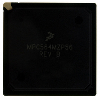
MPC564MZP56 Freescale Semiconductor, MPC564MZP56 Datasheet - Page 44

MPC564MZP56
Manufacturer Part Number
MPC564MZP56
Description
IC MCU 512K FLASH 56MHZ 388-BGA
Manufacturer
Freescale Semiconductor
Series
MPC5xxr
Specifications of MPC564MZP56
Core Processor
PowerPC
Core Size
32-Bit
Speed
56MHz
Connectivity
CAN, EBI/EMI, SCI, SPI, UART/USART
Peripherals
POR, PWM, WDT
Number Of I /o
56
Program Memory Size
512KB (512K x 8)
Program Memory Type
FLASH
Ram Size
32K x 8
Voltage - Supply (vcc/vdd)
2.5 V ~ 2.7 V
Data Converters
A/D 32x10b
Oscillator Type
External
Operating Temperature
-40°C ~ 125°C
Package / Case
388-BGA
Core
PowerPC
Processor Series
MPC5xx
Data Bus Width
32 bit
Maximum Clock Frequency
56 MHz
Data Ram Size
32 KB
On-chip Adc
Yes
Number Of Programmable I/os
56
Number Of Timers
2
Operating Supply Voltage
0 V to 5 V
Mounting Style
SMD/SMT
A/d Bit Size
10 bit
A/d Channels Available
32
Height
1.95 mm
Interface Type
CAN, JTAG, QSPI, SCI, SPI, UART
Length
27 mm
Maximum Operating Temperature
+ 125 C
Minimum Operating Temperature
- 40 C
Supply Voltage (max)
2.7 V, 5.25 V
Supply Voltage (min)
2.5 V, 4.75 V
Width
27 mm
For Use With
MPC564EVB - KIT EVAL FOR MPC561/562/563/564
Lead Free Status / RoHS Status
Contains lead / RoHS non-compliant
Eeprom Size
-
Lead Free Status / Rohs Status
No RoHS Version Available
Available stocks
Company
Part Number
Manufacturer
Quantity
Price
Company:
Part Number:
MPC564MZP56
Manufacturer:
FREESCAL
Quantity:
364
Company:
Part Number:
MPC564MZP56
Manufacturer:
Freescale Semiconductor
Quantity:
10 000
Part Number:
MPC564MZP56
Manufacturer:
FREESCALE
Quantity:
20 000
Company:
Part Number:
MPC564MZP56R2
Manufacturer:
Freescale Semiconductor
Quantity:
10 000
- Current page: 44 of 1420
- Download datasheet (11Mb)
9-9
9-10
9-11
9-12
9-13
9-14
9-15
9-16
9-17
9-18
9-19
9-20
9-21
9-22
9-23
9-24
9-25
9-26
9-27
9-28
9-29
9-30
9-31
9-32
9-33
9-34
9-35
9-36
9-37
9-38
9-39
9-40
9-41
9-42
10-1
10-2
10-3
10-4
10-5
xliv
Figure
Number
Single Beat Basic Write Cycle Timing – One Wait State ...................................................... 9-14
Single Beat 32-Bit Data Write Cycle Timing — 16-Bit Port Size ......................................... 9-15
Read Followed by Write when Pre-Discharge Mode is Enabled, and EHTR is Set .............. 9-17
Basic Flow Diagram Of A Burst-Read Cycle......................................................................... 9-21
Burst-Read Cycle – 32-Bit Port Size – Zero Wait State......................................................... 9-21
Burst-Read Cycle – 32-Bit Port Size – One Wait State.......................................................... 9-22
Burst-Read Cycle – 32-Bit Port Size – Wait States Between Beats ....................................... 9-23
Burst-Read Cycle – 16-Bit Port Size ...................................................................................... 9-24
Basic Flow Diagram of a Burst-Write Cycle.......................................................................... 9-26
Burst-Write Cycle, 32-Bit Port Size, Zero Wait States
(Only for External Master Memory Controller Service Support)........................................... 9-26
Burst-Inhibit Read Cycle, 32-Bit Port Size (Emulated Burst)................................................ 9-27
Non-Wrap Burst with Three Beats ......................................................................................... 9-28
Non-Wrap Burst with One Data Beat ..................................................................................... 9-29
Internal Operand Representation ............................................................................................ 9-30
Interface To Different Port Size Devices................................................................................ 9-31
Bus Arbitration Flowchart ...................................................................................................... 9-33
Master Signals Basic Connection ........................................................................................... 9-34
Bus Arbitration Timing Diagram............................................................................................ 9-35
Internal Bus Arbitration State Machine .................................................................................. 9-36
Termination Signals Protocol Basic Connection .................................................................... 9-41
Termination Signals Protocol Timing Diagram...................................................................... 9-41
Reservation on Local Bus ....................................................................................................... 9-43
Reservation on Multi-level Bus Hierarchy ............................................................................. 9-44
Retry Transfer Timing – Internal Arbiter ............................................................................... 9-46
Retry Transfer Timing – External Arbiter .............................................................................. 9-47
Retry on Burst Cycle............................................................................................................... 9-48
Basic Flow of an External Master Read Access ..................................................................... 9-50
Basic Flow of an External Master Write Access .................................................................... 9-51
Peripheral Mode: External Master Reads from MPC561/MPC563 (Two Wait States) ......... 9-52
Peripheral Mode: External Master Writes to MPC561/MPC563 (Two Wait States)............ 9-53
Flow of Retry of External Master Read Access ..................................................................... 9-54
Retry of External Master Access (Internal Arbiter)................................................................ 9-55
Instruction Show Cycle Transaction....................................................................................... 9-57
Data Show Cycle Transaction................................................................................................. 9-58
Memory Controller Function within the USIU....................................................................... 10-1
Memory Controller Block Diagram........................................................................................ 10-2
MPC561/MPC563 Simple System Configuration .................................................................. 10-3
Bank Base Address and Match Structure ............................................................................... 10-4
A 4-2-2-2 Burst Read Cycle (One Wait State Between Bursts) ............................................. 10-9
MPC561/MPC563 Reference Manual, Rev. 1.2
Figures
Title
Freescale Semiconductor
Number
Page
Related parts for MPC564MZP56
Image
Part Number
Description
Manufacturer
Datasheet
Request
R

Part Number:
Description:
MPC5 1K0 5%
Manufacturer:
TE Connectivity
Datasheet:

Part Number:
Description:
MPC5 500R 5%
Manufacturer:
TE Connectivity
Datasheet:

Part Number:
Description:
MPC5 5K0 5%
Manufacturer:
Tyco Electronics
Datasheet:

Part Number:
Description:
MPC5 5R0 5%
Manufacturer:
Tyco Electronics
Datasheet:

Part Number:
Description:
MPC5 50K 5%
Manufacturer:
Tyco Electronics
Datasheet:

Part Number:
Description:
MPC5 1R0 5%
Manufacturer:
Tyco Electronics
Datasheet:
Part Number:
Description:
Manufacturer:
Freescale Semiconductor, Inc
Datasheet:
Part Number:
Description:
Manufacturer:
Freescale Semiconductor, Inc
Datasheet:
Part Number:
Description:
Manufacturer:
Freescale Semiconductor, Inc
Datasheet:
Part Number:
Description:
Manufacturer:
Freescale Semiconductor, Inc
Datasheet:
Part Number:
Description:
Manufacturer:
Freescale Semiconductor, Inc
Datasheet:


