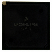
MPC564MZP56 Freescale Semiconductor, MPC564MZP56 Datasheet - Page 1030

MPC564MZP56
Manufacturer Part Number
MPC564MZP56
Description
IC MCU 512K FLASH 56MHZ 388-BGA
Manufacturer
Freescale Semiconductor
Series
MPC5xxr
Specifications of MPC564MZP56
Core Processor
PowerPC
Core Size
32-Bit
Speed
56MHz
Connectivity
CAN, EBI/EMI, SCI, SPI, UART/USART
Peripherals
POR, PWM, WDT
Number Of I /o
56
Program Memory Size
512KB (512K x 8)
Program Memory Type
FLASH
Ram Size
32K x 8
Voltage - Supply (vcc/vdd)
2.5 V ~ 2.7 V
Data Converters
A/D 32x10b
Oscillator Type
External
Operating Temperature
-40°C ~ 125°C
Package / Case
388-BGA
Core
PowerPC
Processor Series
MPC5xx
Data Bus Width
32 bit
Maximum Clock Frequency
56 MHz
Data Ram Size
32 KB
On-chip Adc
Yes
Number Of Programmable I/os
56
Number Of Timers
2
Operating Supply Voltage
0 V to 5 V
Mounting Style
SMD/SMT
A/d Bit Size
10 bit
A/d Channels Available
32
Height
1.95 mm
Interface Type
CAN, JTAG, QSPI, SCI, SPI, UART
Length
27 mm
Maximum Operating Temperature
+ 125 C
Minimum Operating Temperature
- 40 C
Supply Voltage (max)
2.7 V, 5.25 V
Supply Voltage (min)
2.5 V, 4.75 V
Width
27 mm
For Use With
MPC564EVB - KIT EVAL FOR MPC561/562/563/564
Lead Free Status / RoHS Status
Contains lead / RoHS non-compliant
Eeprom Size
-
Lead Free Status / Rohs Status
No RoHS Version Available
Available stocks
Company
Part Number
Manufacturer
Quantity
Price
Company:
Part Number:
MPC564MZP56
Manufacturer:
FREESCAL
Quantity:
364
Company:
Part Number:
MPC564MZP56
Manufacturer:
Freescale Semiconductor
Quantity:
10 000
Part Number:
MPC564MZP56
Manufacturer:
FREESCALE
Quantity:
20 000
Company:
Part Number:
MPC564MZP56R2
Manufacturer:
Freescale Semiconductor
Quantity:
10 000
- Current page: 1030 of 1420
- Download datasheet (11Mb)
READI Module
24.10.2.2 Block Write Operation
For a block write access to memory-mapped locations, the following sequence of operations need to be
performed via the auxiliary port:
24-62
2. The download request public message contains:
3. After completion of the write operation, the device ready for upload/download public message
4. The SC bit is cleared to indicate that the write access is complete.
1. The tool confirms that the device is ready before transmitting download request public message
2. The download request public message contains:
3. After completion of this write operation, the device ready for upload/download public message
a) TCODE(18)
b) Access opcode 0xF which signals that subsequent data needs to be stored in the RWA register.
c) Configure the RWA register fields as follows:
(TCODE=16) is transmitted to the tool indicating that the device is ready for next access.
(TCODE = 18).
a) TCODE(18)
b) Access opcode 0xF which signals that subsequent data needs to be stored in the RWA register.
c) Configure the RWA register fields as follows
(TCODE = 16) is transmitted to the tool indicating that the device is ready for next access.
– Start/complete (1 to indicate start access) -> SC
– Read/write address (write address) -> RWAD
– Read/write (1 to indicate a write access) -> RW
– Word size (32 bits, 16 bits, 8 bits) -> SZ
– Write data (write data) -> WD
– Privilege (user data/instruction, supervisor data/instruction) -> PRV
– Map select (select memory map, 0b0 or 0b1) -> MAP
– Access Count (0 to indicate single access) -> CNT
– Start/complete (1 to indicate start access) -> SC
– Read/write address (starting write address of block) -> RWAD
– Read/write (1 to indicate a write access) -> RW
– Word size (32 bits, 16 bits, 8 bits) -> SZ
– Write data (write data) -> WD
– Privilege (user data/instruction, supervisor data/instruction) -> PRV
– Map select (select memory map 0b0) -> MAP
– Access count (non zero number to indicate size of block access) -> CNT
0 = Normal memory access
1 = Secondary memory map (SPR)
MPC561/MPC563 Reference Manual, Rev. 1.2
Freescale Semiconductor
Related parts for MPC564MZP56
Image
Part Number
Description
Manufacturer
Datasheet
Request
R

Part Number:
Description:
MPC5 1K0 5%
Manufacturer:
TE Connectivity
Datasheet:

Part Number:
Description:
MPC5 500R 5%
Manufacturer:
TE Connectivity
Datasheet:

Part Number:
Description:
MPC5 5K0 5%
Manufacturer:
Tyco Electronics
Datasheet:

Part Number:
Description:
MPC5 5R0 5%
Manufacturer:
Tyco Electronics
Datasheet:

Part Number:
Description:
MPC5 50K 5%
Manufacturer:
Tyco Electronics
Datasheet:

Part Number:
Description:
MPC5 1R0 5%
Manufacturer:
Tyco Electronics
Datasheet:
Part Number:
Description:
Manufacturer:
Freescale Semiconductor, Inc
Datasheet:
Part Number:
Description:
Manufacturer:
Freescale Semiconductor, Inc
Datasheet:
Part Number:
Description:
Manufacturer:
Freescale Semiconductor, Inc
Datasheet:
Part Number:
Description:
Manufacturer:
Freescale Semiconductor, Inc
Datasheet:
Part Number:
Description:
Manufacturer:
Freescale Semiconductor, Inc
Datasheet:


