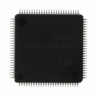
M30833FJGP#U5 Renesas Electronics America, M30833FJGP#U5 Datasheet - Page 40

M30833FJGP#U5
Manufacturer Part Number
M30833FJGP#U5
Description
IC M32C/83 MCU FLASH 100LQFP
Manufacturer
Renesas Electronics America
Series
M16C™ M32C/80r
Datasheets
1.M3087BFLGPU3.pdf
(364 pages)
2.M30833FJGPU3.pdf
(96 pages)
3.M30833FJGPU3.pdf
(529 pages)
Specifications of M30833FJGP#U5
Core Processor
M32C/80
Core Size
16/32-Bit
Speed
32MHz
Connectivity
CAN, I²C, IEBus, SIO, UART/USART
Peripherals
DMA, WDT
Number Of I /o
85
Program Memory Size
512KB (512K x 8)
Program Memory Type
FLASH
Ram Size
31K x 8
Voltage - Supply (vcc/vdd)
3 V ~ 5.5 V
Data Converters
A/D 26x10b; D/A 2x8b
Oscillator Type
Internal
Operating Temperature
-20°C ~ 85°C
Package / Case
100-LQFP
For Use With
R0K330879S001BE - KIT DEV RSK M32C/87R0K330879S000BE - KIT DEV RSK M32C/87
Lead Free Status / RoHS Status
Lead free / RoHS Compliant
Eeprom Size
-
Available stocks
Company
Part Number
Manufacturer
Quantity
Price
Part Number:
M30833FJGP#U5M30833FJGP#U3
Manufacturer:
Renesas Electronics America
Quantity:
10 000
- Current page: 40 of 529
- Download datasheet (5Mb)
R
R
M
e
E
3
. v
J
2
I : Input
NOTE:
0
_______
Table 1.6 Pin Description (100-Pin and 144-Pin Packages) (Continued)
Main Clock Input
Main Clock Output
Sub Clock Input
Sub Clock Output
Low-Pass Filter
Connect
Pin for PLL
Frequency
Synthesizer Pin
BCLK Output
Clock Output
______
INT Interrupt Input
NMI Interrupt Input
Key Input Interrupt
Timer A
Timer B
Three-phase Motor
Control Timer Output
Serial I/O
I
C
Classsfication
1
2
9
C Mode
3 .
B
8 /
1. Bus control pins in M32C/83T cannot be used.
0
1
3
0
3
G
J
4
a
o r
0 -
n
3 .
u
1
O : Output
p
, 1
3
1
(1)
(
2
M
0
_______
3
X
X
X
X
V
BCLK
CLK
________
INT0 to INT5
NMI
_____
KI
TA0
TA4
TA0
TA4
TB0
TB5
U, U, V, V,
W, W
CTS0 to CTS4
RTS0 to RTS4
CLK0 to CLK4
RxD0 to RxD4
TxD0 to TxD4
SDA0 to
SDA4
SCL0 to
SCL4
0
_________
_________
6
2
IN
OUT
CIN
COUT
CONT
Symbol
0
C
___
___
to KI
OUT
OUT
IN
IN
IN
IN
OUT
8 /
Page 15
_____
, 3
to
to
________
_________
________
___
3
to
M
I/O : Input and output
3
2
I/O Type
C
I/O
I/O
I/O
f o
O
O
O
O
O
O
O
8 /
I
I
I
I
I
I
I
I
I
4
3
8
) T
8
I/O pins for the main clock oscillation circuit. Connect a ceramic resonator
or crystal oscillator between X
to X
I/O pins for the sub clock oscillation circuit. Connect a crystal oscillator
between X
leave X
Connects the low-pass filter to the VCONT pin when using the PLL fre-
quency synthesizer. Connect P8
Outputs BCLK signal
Outputs the clock having the same frequency as f
Input pins for the INT interrupt
Input pin for the NMI interrupt
Input pins for the key input interrupt
I/O pins for the timer A0 to A4
(TA0
Input pins for the timer A0 to A4
Input pins for the timer B0 to B5
Output pins for the three-phase motor control timer
Input pins for data transmission control
Output pins for data reception control
Inputs and outputs the transfer clock
Inputs serial data
Outputs serial data
(TxD2 is a pin for the N-channel open drain output.)
Inputs and outputs serial data
(SDA2 is a pin for the N-channel open drain output.)
Inputs and outputs the transfer clock
(SCL2 is a pin for the N-channel open drain output.)
IN
OUT
and leave X
COUT
is a pin for the N-channel open drain output.)
CIN
open
and X
_______
______
OUT
COUT
open
. To apply external clock, apply it to X
Function
IN
6
and X
to VSS to stabilize the PLL frequency.
OUT
. To apply external clock, apply it
C
, f
8
or f
32
CIN
1. Overview
and
Related parts for M30833FJGP#U5
Image
Part Number
Description
Manufacturer
Datasheet
Request
R

Part Number:
Description:
KIT STARTER FOR M16C/29
Manufacturer:
Renesas Electronics America
Datasheet:

Part Number:
Description:
KIT STARTER FOR R8C/2D
Manufacturer:
Renesas Electronics America
Datasheet:

Part Number:
Description:
R0K33062P STARTER KIT
Manufacturer:
Renesas Electronics America
Datasheet:

Part Number:
Description:
KIT STARTER FOR R8C/23 E8A
Manufacturer:
Renesas Electronics America
Datasheet:

Part Number:
Description:
KIT STARTER FOR R8C/25
Manufacturer:
Renesas Electronics America
Datasheet:

Part Number:
Description:
KIT STARTER H8S2456 SHARPE DSPLY
Manufacturer:
Renesas Electronics America
Datasheet:

Part Number:
Description:
KIT STARTER FOR R8C38C
Manufacturer:
Renesas Electronics America
Datasheet:

Part Number:
Description:
KIT STARTER FOR R8C35C
Manufacturer:
Renesas Electronics America
Datasheet:

Part Number:
Description:
KIT STARTER FOR R8CL3AC+LCD APPS
Manufacturer:
Renesas Electronics America
Datasheet:

Part Number:
Description:
KIT STARTER FOR RX610
Manufacturer:
Renesas Electronics America
Datasheet:

Part Number:
Description:
KIT STARTER FOR R32C/118
Manufacturer:
Renesas Electronics America
Datasheet:

Part Number:
Description:
KIT DEV RSK-R8C/26-29
Manufacturer:
Renesas Electronics America
Datasheet:

Part Number:
Description:
KIT STARTER FOR SH7124
Manufacturer:
Renesas Electronics America
Datasheet:

Part Number:
Description:
KIT STARTER FOR H8SX/1622
Manufacturer:
Renesas Electronics America
Datasheet:

Part Number:
Description:
KIT DEV FOR SH7203
Manufacturer:
Renesas Electronics America
Datasheet:


