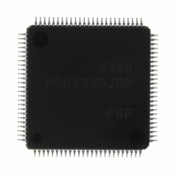
M30833FJGP#U5 Renesas Electronics America, M30833FJGP#U5 Datasheet - Page 387

M30833FJGP#U5
Manufacturer Part Number
M30833FJGP#U5
Description
IC M32C/83 MCU FLASH 100LQFP
Manufacturer
Renesas Electronics America
Series
M16C™ M32C/80r
Datasheets
1.M3087BFLGPU3.pdf
(364 pages)
2.M30833FJGPU3.pdf
(96 pages)
3.M30833FJGPU3.pdf
(529 pages)
Specifications of M30833FJGP#U5
Core Processor
M32C/80
Core Size
16/32-Bit
Speed
32MHz
Connectivity
CAN, I²C, IEBus, SIO, UART/USART
Peripherals
DMA, WDT
Number Of I /o
85
Program Memory Size
512KB (512K x 8)
Program Memory Type
FLASH
Ram Size
31K x 8
Voltage - Supply (vcc/vdd)
3 V ~ 5.5 V
Data Converters
A/D 26x10b; D/A 2x8b
Oscillator Type
Internal
Operating Temperature
-20°C ~ 85°C
Package / Case
100-LQFP
For Use With
R0K330879S001BE - KIT DEV RSK M32C/87R0K330879S000BE - KIT DEV RSK M32C/87
Lead Free Status / RoHS Status
Lead free / RoHS Compliant
Eeprom Size
-
Available stocks
Company
Part Number
Manufacturer
Quantity
Price
Part Number:
M30833FJGP#U5M30833FJGP#U3
Manufacturer:
Renesas Electronics America
Quantity:
10 000
- Current page: 387 of 529
- Download datasheet (5Mb)
R
R
M
e
E
3
. v
J
Figure 23.2 Multiplexed Address Output Pattern
2
0
1
C
9
3 .
B
8 /
(2) In 16-bit Bus Mode
(1) In 8-bit Bus Mode
0
1
3
0
3
J
G
4
a
0 -
n
o r
Row Address
Row Address
Row Address
Row Address
Row Address
Row Address
Pin Function
Column Address
Column Address
Column Address
Pin Function
Column Address
Column Address
Column Address
3 .
1
u
NOTES:
, 1
3
p
1
1. The above applies when using a 4Mx1 or 4Mx4 memory configuration. When using a 4Mx16
2
(
M
0
0
( ): disabled bits,
configuration, implement the following combinations:
For row addresses, MA0 to MA12; for column addresses, MA2 to MA8, MA11 and MA12.
Or for row addresses, MA1 to MA12; for column addresses, MA2 to MA9, MA11 and MA12.
–: indetermimate
3
6
2
C
Page 362
8 /
, 3
M
(A20)
MA12 MA11 MA10
(A20)
(A22)
(A20)
(A22)
(A22)
MA12 MA11 MA10
(A20)
(A22)
(A20)
(A20)
(A22)
A20
A20
A22
3
2
C
f o
DRAM area
8 /
(A19)
(A19)
(A22)
(A19)
(A20)
(A19)
4
A19
A21
A19
A21
A22
A19
A20
A19
3
8
) T
8
Address used for 4M-byte and 8M-byte
(A18)
(A18) (A17)
:bits which output addresses changed by data bus width and the
A19
A18
A21
A18
A18
A18
A20
A18
A18
A9
A9
A9
Address used for 1M-byte and 2M-byte DRAM area
Address used for 2M-byte and 4M-byte DRAM area
Address used for 512K-byte and 1M-byte DRAM area
(A17)
MA9
MA9
A17
A17
A17
A17
A17
A17
A8
A8
A8
Address used for 8M-byte DRAM area
A8
A8
A8
Address used for 512K-byte DRAM area
(A16)
(A16)
MA8
MA8
A16
A16
A16
A16
A16
A16
A7
A7
A7
A7
A7
A7
(A15) (A14)
(A15)
MA7
MA7
A15
A15
A15
A15
A15
A15
A6
A6
A6
A6
A6
A6
(A14) (A13)
MA6
MA6
A14
A14
A14
A14
A14
A14
A5
A5
A5
A5
A5
A5
(A13)
MA5
MA5
A13
A13
A13
A13
A13
A13
(1)
A4
A4
A4
A4
A4
A4
DRAM area
(A12) (A11)
(A12)
MA4
MA4
A12
A12
A12
A12
A12
A12
A3
A3
A3
A3
A3
A3
(A11) (A10)
MA3
MA3
A11
A11
A11
A11
A11
A11
A2
A2
A2
A2
A2
A2
(A10)
MA2
MA2
A10
A10
A10
A10
A10
A10
A1
A1
A1
A1
A1
A1
MA1
MA1
(A9)
(A9)
(A9)
(A0)
(A9)
(A0)
(A9)
(A0)
A9
A0
A9
A0
A9
A0
MA0
MA0
(A8)
(A8)
23. DRAMC
–
–
–
–
–
–
–
–
–
–
–
–
Related parts for M30833FJGP#U5
Image
Part Number
Description
Manufacturer
Datasheet
Request
R

Part Number:
Description:
KIT STARTER FOR M16C/29
Manufacturer:
Renesas Electronics America
Datasheet:

Part Number:
Description:
KIT STARTER FOR R8C/2D
Manufacturer:
Renesas Electronics America
Datasheet:

Part Number:
Description:
R0K33062P STARTER KIT
Manufacturer:
Renesas Electronics America
Datasheet:

Part Number:
Description:
KIT STARTER FOR R8C/23 E8A
Manufacturer:
Renesas Electronics America
Datasheet:

Part Number:
Description:
KIT STARTER FOR R8C/25
Manufacturer:
Renesas Electronics America
Datasheet:

Part Number:
Description:
KIT STARTER H8S2456 SHARPE DSPLY
Manufacturer:
Renesas Electronics America
Datasheet:

Part Number:
Description:
KIT STARTER FOR R8C38C
Manufacturer:
Renesas Electronics America
Datasheet:

Part Number:
Description:
KIT STARTER FOR R8C35C
Manufacturer:
Renesas Electronics America
Datasheet:

Part Number:
Description:
KIT STARTER FOR R8CL3AC+LCD APPS
Manufacturer:
Renesas Electronics America
Datasheet:

Part Number:
Description:
KIT STARTER FOR RX610
Manufacturer:
Renesas Electronics America
Datasheet:

Part Number:
Description:
KIT STARTER FOR R32C/118
Manufacturer:
Renesas Electronics America
Datasheet:

Part Number:
Description:
KIT DEV RSK-R8C/26-29
Manufacturer:
Renesas Electronics America
Datasheet:

Part Number:
Description:
KIT STARTER FOR SH7124
Manufacturer:
Renesas Electronics America
Datasheet:

Part Number:
Description:
KIT STARTER FOR H8SX/1622
Manufacturer:
Renesas Electronics America
Datasheet:

Part Number:
Description:
KIT DEV FOR SH7203
Manufacturer:
Renesas Electronics America
Datasheet:


