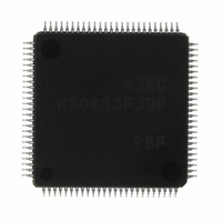
M30833FJGP#U5 Renesas Electronics America, M30833FJGP#U5 Datasheet - Page 290

M30833FJGP#U5
Manufacturer Part Number
M30833FJGP#U5
Description
IC M32C/83 MCU FLASH 100LQFP
Manufacturer
Renesas Electronics America
Series
M16C™ M32C/80r
Datasheets
1.M3087BFLGPU3.pdf
(364 pages)
2.M30833FJGPU3.pdf
(96 pages)
3.M30833FJGPU3.pdf
(529 pages)
Specifications of M30833FJGP#U5
Core Processor
M32C/80
Core Size
16/32-Bit
Speed
32MHz
Connectivity
CAN, I²C, IEBus, SIO, UART/USART
Peripherals
DMA, WDT
Number Of I /o
85
Program Memory Size
512KB (512K x 8)
Program Memory Type
FLASH
Ram Size
31K x 8
Voltage - Supply (vcc/vdd)
3 V ~ 5.5 V
Data Converters
A/D 26x10b; D/A 2x8b
Oscillator Type
Internal
Operating Temperature
-20°C ~ 85°C
Package / Case
100-LQFP
For Use With
R0K330879S001BE - KIT DEV RSK M32C/87R0K330879S000BE - KIT DEV RSK M32C/87
Lead Free Status / RoHS Status
Lead free / RoHS Compliant
Eeprom Size
-
Available stocks
Company
Part Number
Manufacturer
Quantity
Price
Part Number:
M30833FJGP#U5M30833FJGP#U3
Manufacturer:
Renesas Electronics America
Quantity:
10 000
- Current page: 290 of 529
- Download datasheet (5Mb)
R
R
M
e
E
3
. v
J
2
0
Table 21.2 Base Timer Specifications (Continued)
Figure 21.16 Base Timer Block Diagram
Table 21.3 Base Timer Associated Register Settings
(for Time Measurement Function, Waveform Generation Function, and Communication Function)
G2BCR0
BTSR
GiBCR0
GiBCR1
GiBT
Set the following registers to set the RST1 bit to "1" (base timer reset by matching the base timer with the G1PO0 register).
GiPOCR0
GiPO0
GiFS
GiFE
i : Bit configurations and functions vary with each group
1
C
9
BTS bit in GiBCR1 register
Selectable Function
Register
3 .
BTiS bit in BTSR register
B
Apply "L" to the INT
8 /
Request from communication
function (Group2,3)
0
1
Matching with the GiPO0 register
3
0
3
J
G
4
a
Apply two-phase
pulse signal (
Group0,1)
0 -
n
o r
3 .
1
u
, 1
3
p
Other base timer reset
1
2
(
Item
M
-
-
BCK1 to BCK0
DIV4 to DIV0
IT
RST2 to RST1
BTS
UD1 to UD0
CAS
-
MOD2 to MOD0
-
FSC0
IFE0
0
0
3
6
i
2
pin (Group0,1)
f
C
1
8 /
Page 265
Bit
, 3
10
11
BCK1 to BCK0
M
3
2
C
f o
8 /
RST0
RST1
RST2
4
Supplies operation clock to the BTSR register. Set to "0111 1111
Set to "0000 0000
Select count source
Select divide ratio of count source
Selects the base timer interrupt
Select factors for a base timer reset
Used to start the base timer independently
Select how to count (Group 0 and 1)
Selects cascaded connection (Group 0 and 1)
Read or write base timer value
Set to "000
Set reset cycle
Set to "0" (waveform generation function)
Set to "1" (channel operation start)
3
8
) T
8
• Two-phase pulse processing mode (Group 0 and 1)
and P8
by 2(n+1)
Divider
Two-phase pulse signals from P7
P7
P7
2
1
" (single-phase waveform output mode)
7
6
(1)
, P8
, P8
pins in group 1 are counted (See Figure 21.20)
NOTES:
i = 0 to 3
BCK1 to BCK0, IT : Bits in the GiBCR0 register
RST2 to RST0 : Bits in the GiBCR1 register
1. Divider is reset when both BTiS bit and BTS bit are set to "0".
1
0
Base timer reset
2
f
BTi
"
The timer increments
counter on all edge
b0 to b13
Base timer
Function
Specification
b14 b15
6
and P7
0
1
The timer decrements
counter on all deges
Overflow signal
IT
7
21. Intelligent I/O (Base Timer)
pins in group 0, and P8
(See the BTiR bit in Figure 10.14)
Base timer
interrupt request
2
".
0
Related parts for M30833FJGP#U5
Image
Part Number
Description
Manufacturer
Datasheet
Request
R

Part Number:
Description:
KIT STARTER FOR M16C/29
Manufacturer:
Renesas Electronics America
Datasheet:

Part Number:
Description:
KIT STARTER FOR R8C/2D
Manufacturer:
Renesas Electronics America
Datasheet:

Part Number:
Description:
R0K33062P STARTER KIT
Manufacturer:
Renesas Electronics America
Datasheet:

Part Number:
Description:
KIT STARTER FOR R8C/23 E8A
Manufacturer:
Renesas Electronics America
Datasheet:

Part Number:
Description:
KIT STARTER FOR R8C/25
Manufacturer:
Renesas Electronics America
Datasheet:

Part Number:
Description:
KIT STARTER H8S2456 SHARPE DSPLY
Manufacturer:
Renesas Electronics America
Datasheet:

Part Number:
Description:
KIT STARTER FOR R8C38C
Manufacturer:
Renesas Electronics America
Datasheet:

Part Number:
Description:
KIT STARTER FOR R8C35C
Manufacturer:
Renesas Electronics America
Datasheet:

Part Number:
Description:
KIT STARTER FOR R8CL3AC+LCD APPS
Manufacturer:
Renesas Electronics America
Datasheet:

Part Number:
Description:
KIT STARTER FOR RX610
Manufacturer:
Renesas Electronics America
Datasheet:

Part Number:
Description:
KIT STARTER FOR R32C/118
Manufacturer:
Renesas Electronics America
Datasheet:

Part Number:
Description:
KIT DEV RSK-R8C/26-29
Manufacturer:
Renesas Electronics America
Datasheet:

Part Number:
Description:
KIT STARTER FOR SH7124
Manufacturer:
Renesas Electronics America
Datasheet:

Part Number:
Description:
KIT STARTER FOR H8SX/1622
Manufacturer:
Renesas Electronics America
Datasheet:

Part Number:
Description:
KIT DEV FOR SH7203
Manufacturer:
Renesas Electronics America
Datasheet:


