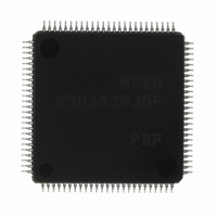
M30833FJGP#U5 Renesas Electronics America, M30833FJGP#U5 Datasheet - Page 131

M30833FJGP#U5
Manufacturer Part Number
M30833FJGP#U5
Description
IC M32C/83 MCU FLASH 100LQFP
Manufacturer
Renesas Electronics America
Series
M16C™ M32C/80r
Datasheets
1.M3087BFLGPU3.pdf
(364 pages)
2.M30833FJGPU3.pdf
(96 pages)
3.M30833FJGPU3.pdf
(529 pages)
Specifications of M30833FJGP#U5
Core Processor
M32C/80
Core Size
16/32-Bit
Speed
32MHz
Connectivity
CAN, I²C, IEBus, SIO, UART/USART
Peripherals
DMA, WDT
Number Of I /o
85
Program Memory Size
512KB (512K x 8)
Program Memory Type
FLASH
Ram Size
31K x 8
Voltage - Supply (vcc/vdd)
3 V ~ 5.5 V
Data Converters
A/D 26x10b; D/A 2x8b
Oscillator Type
Internal
Operating Temperature
-20°C ~ 85°C
Package / Case
100-LQFP
For Use With
R0K330879S001BE - KIT DEV RSK M32C/87R0K330879S000BE - KIT DEV RSK M32C/87
Lead Free Status / RoHS Status
Lead free / RoHS Compliant
Eeprom Size
-
Available stocks
Company
Part Number
Manufacturer
Quantity
Price
Part Number:
M30833FJGP#U5M30833FJGP#U3
Manufacturer:
Renesas Electronics America
Quantity:
10 000
- Current page: 131 of 529
- Download datasheet (5Mb)
R
R
M
10.8 NMI Interrupt
10.9 Key Input Interrupt
e
E
3
. v
J
Figure 10.11 Key Input Interrupt
2
0
The NMI interrupt occurs when the signal applied to the P8
signal. The NMI interrupt is a non-maskable interrupt. Although the P8
rupt input pin, the P8_5 bit in the P8
Key input interrupt request is generated when one of the signals applied to the P10
mode is on the falling edge. The key input interrupt can be also used as key-on wake-up function to exit wait
or stop mode. To use the key input interrupt, do not use P10
shows a block diagram of the key input interrupt. When an "L" signal is applied to any pins in input mode,
signals applied to other pins are not detected as a request signal for an interrupt.
When the PSC_7 bit in the PSC register
occurs regardless of interrupt control register settings. When the PSC_7 bit is set to "1", no input from a
port pin is available even when in input mode.
NOTES:
1
9
C
3 .
B
NOTES:
When the NMI interrupt is not used, connect (pull-up) the NMI pin to Vcc via a resistor. Because the NMI
interrupt cannot be ignored, the pin must be connected.
1. Refer to 24. Programmable I/O Ports for details on the PSC register.
8 /
0
1
______
3
0
______
3
J
G
4
a
P10
P10
P10
P10
Pull-up
transistor
0 -
n
o r
3 .
1
u
7
6
5
4
, 1
3
/KI
/KI
/KI
/KI
p
1
______
______
3
2
1
2
0
(
M
0
0
3
6
Pull-up
transistor
2
Pull-up
transistor
Pull-up
transistor
C
8 /
Page 106
, 3
M
PSC_7 bit
3
2
C
f o
8 /
4
3
8
) T
8
PD10_7 bit
PD10_6 bit
PD10_5 bit
PD10_4 bit
5
PD10_7 bit
PU31 bit in PUR3 register
register indicates input level for this pin.
(1)
is set to "1" (key input interrupt disabled), no key input interrupt
5
______
/NMI pin changes from an "H" signal to an "L"
______
4
to P10
KUPIC Register
Interrupt Control
Circuit
7
5
/NMI pin is used as the NMI inter-
as A/D input ports. Figure 10.11
______
4
Key Input Interrupt
Request
to P10
7
pins in input
10. Interrupts
______
______
Related parts for M30833FJGP#U5
Image
Part Number
Description
Manufacturer
Datasheet
Request
R

Part Number:
Description:
KIT STARTER FOR M16C/29
Manufacturer:
Renesas Electronics America
Datasheet:

Part Number:
Description:
KIT STARTER FOR R8C/2D
Manufacturer:
Renesas Electronics America
Datasheet:

Part Number:
Description:
R0K33062P STARTER KIT
Manufacturer:
Renesas Electronics America
Datasheet:

Part Number:
Description:
KIT STARTER FOR R8C/23 E8A
Manufacturer:
Renesas Electronics America
Datasheet:

Part Number:
Description:
KIT STARTER FOR R8C/25
Manufacturer:
Renesas Electronics America
Datasheet:

Part Number:
Description:
KIT STARTER H8S2456 SHARPE DSPLY
Manufacturer:
Renesas Electronics America
Datasheet:

Part Number:
Description:
KIT STARTER FOR R8C38C
Manufacturer:
Renesas Electronics America
Datasheet:

Part Number:
Description:
KIT STARTER FOR R8C35C
Manufacturer:
Renesas Electronics America
Datasheet:

Part Number:
Description:
KIT STARTER FOR R8CL3AC+LCD APPS
Manufacturer:
Renesas Electronics America
Datasheet:

Part Number:
Description:
KIT STARTER FOR RX610
Manufacturer:
Renesas Electronics America
Datasheet:

Part Number:
Description:
KIT STARTER FOR R32C/118
Manufacturer:
Renesas Electronics America
Datasheet:

Part Number:
Description:
KIT DEV RSK-R8C/26-29
Manufacturer:
Renesas Electronics America
Datasheet:

Part Number:
Description:
KIT STARTER FOR SH7124
Manufacturer:
Renesas Electronics America
Datasheet:

Part Number:
Description:
KIT STARTER FOR H8SX/1622
Manufacturer:
Renesas Electronics America
Datasheet:

Part Number:
Description:
KIT DEV FOR SH7203
Manufacturer:
Renesas Electronics America
Datasheet:


