DF2506BR26DV Renesas Electronics America, DF2506BR26DV Datasheet - Page 459
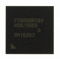
DF2506BR26DV
Manufacturer Part Number
DF2506BR26DV
Description
IC H8S/2506 MCU FLASH 176-LFBGA
Manufacturer
Renesas Electronics America
Series
H8® H8S/2500r
Specifications of DF2506BR26DV
Core Processor
H8S/2000
Core Size
16-Bit
Speed
26MHz
Connectivity
I²C, SCI
Peripherals
POR, PWM, WDT
Number Of I /o
104
Program Memory Size
512KB (512K x 8)
Program Memory Type
FLASH
Ram Size
32K x 8
Voltage - Supply (vcc/vdd)
3 V ~ 5.5 V
Data Converters
A/D 16x10b; D/A 2x8b
Oscillator Type
Internal
Operating Temperature
-40°C ~ 85°C
Package / Case
176-LFBGA
Lead Free Status / RoHS Status
Lead free / RoHS Compliant
Eeprom Size
-
Available stocks
Company
Part Number
Manufacturer
Quantity
Price
Company:

Part Number:
DF2506BR26DV
Manufacturer:
Renesas Electronics America
Quantity:
10 000


Bit
5
4
Bit Name
ORER
FER
Initial
Value
0
0
R/W
R/(W)*
R/(W)*
1
1
Description
Overrun Error
Indicates that an overrun error occurred during reception,
causing abnormal termination.
[Setting condition]
•
The receive data prior to the overrun error is retained in
RDR, and the data received subsequently is lost. Also,
subsequent serial reception cannot be continued while
the ORER flag is set to 1. In clocked synchronous mode,
serial transmission cannot be continued either.
[Clearing condition]
•
The ORER flag is not affected and retains its previous
state when the RE bit in SCR is cleared to 0.
Framing Error
Indicates that a framing error occurred during reception in
asynchronous mode, causing abnormal termination.
[Setting condition]
•
In 2 stop bit mode, only the first stop bit is checked for a
value to 1; the second stop bit is not checked. If a
framing error occurs, the receive data is transferred to
RDR but the RDRF flag is not set. Also, subsequent
serial reception cannot be continued while the FER flag is
set to 1. In clocked synchronous mode, serial
transmission cannot be continued, either.
[Clearing condition]
•
In 2-stop-bit mode, only the first stop bit is checked.
The FER flag is not affected and retains its previous state
when the RE bit in SCR is cleared to 0.
When the next serial reception is completed while
RDRF = 1
When 0 is written to ORER after reading ORER = 1*
When the stop bit is 0
When 0 is written to FER after reading FER = 1*
Section 13 Serial Communication Interface (SCI)
Rev. 6.00 Sep. 24, 2009 Page 411 of 928
REJ09B0099-0600
3
3
Related parts for DF2506BR26DV
Image
Part Number
Description
Manufacturer
Datasheet
Request
R

Part Number:
Description:
KIT STARTER FOR M16C/29
Manufacturer:
Renesas Electronics America
Datasheet:

Part Number:
Description:
KIT STARTER FOR R8C/2D
Manufacturer:
Renesas Electronics America
Datasheet:

Part Number:
Description:
R0K33062P STARTER KIT
Manufacturer:
Renesas Electronics America
Datasheet:

Part Number:
Description:
KIT STARTER FOR R8C/23 E8A
Manufacturer:
Renesas Electronics America
Datasheet:

Part Number:
Description:
KIT STARTER FOR R8C/25
Manufacturer:
Renesas Electronics America
Datasheet:

Part Number:
Description:
KIT STARTER H8S2456 SHARPE DSPLY
Manufacturer:
Renesas Electronics America
Datasheet:

Part Number:
Description:
KIT STARTER FOR R8C38C
Manufacturer:
Renesas Electronics America
Datasheet:

Part Number:
Description:
KIT STARTER FOR R8C35C
Manufacturer:
Renesas Electronics America
Datasheet:

Part Number:
Description:
KIT STARTER FOR R8CL3AC+LCD APPS
Manufacturer:
Renesas Electronics America
Datasheet:
Part Number:
Description:
KIT STARTER FOR RX610
Manufacturer:
Renesas Electronics America
Datasheet:

Part Number:
Description:
KIT STARTER FOR R32C/118
Manufacturer:
Renesas Electronics America
Datasheet:

Part Number:
Description:
KIT DEV RSK-R8C/26-29
Manufacturer:
Renesas Electronics America
Datasheet:

Part Number:
Description:
KIT STARTER FOR SH7124
Manufacturer:
Renesas Electronics America
Datasheet:

Part Number:
Description:
KIT STARTER FOR H8SX/1622
Manufacturer:
Renesas Electronics America
Datasheet:

Part Number:
Description:
KIT DEV FOR SH7203
Manufacturer:
Renesas Electronics America
Datasheet: