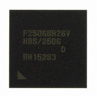
DF2506BR26DV Renesas Electronics America, DF2506BR26DV Datasheet - Page 194

DF2506BR26DV
Manufacturer Part Number
DF2506BR26DV
Description
IC H8S/2506 MCU FLASH 176-LFBGA
Manufacturer
Renesas Electronics America
Series
H8® H8S/2500r
Specifications of DF2506BR26DV
Core Processor
H8S/2000
Core Size
16-Bit
Speed
26MHz
Connectivity
I²C, SCI
Peripherals
POR, PWM, WDT
Number Of I /o
104
Program Memory Size
512KB (512K x 8)
Program Memory Type
FLASH
Ram Size
32K x 8
Voltage - Supply (vcc/vdd)
3 V ~ 5.5 V
Data Converters
A/D 16x10b; D/A 2x8b
Oscillator Type
Internal
Operating Temperature
-40°C ~ 85°C
Package / Case
176-LFBGA
Lead Free Status / RoHS Status
Lead free / RoHS Compliant
Eeprom Size
-
Available stocks
Company
Part Number
Manufacturer
Quantity
Price
Company:
Part Number:
DF2506BR26DV
Manufacturer:
Renesas Electronics America
Quantity:
10 000
- Current page: 194 of 980
- Download datasheet (6Mb)
Section 7 Bus Controller
7.6.2
Table 7.3 shows the data buses used and valid strobes for the access spaces.
In read access, the RD signal is valid without discrimination between the upper and lower halves
of the data bus.
In write access, the HWR signal is valid for the upper half of the data bus, and the LWR signal for
the lower half.
Table 7.3
Legend:
Hi-Z:
Invalid: Input state; input value is ignored.
Rev. 6.00 Sep. 24, 2009 Page 146 of 928
REJ09B0099-0600
Area
8-bit access
space
16-bit
access
space
High impedance
Figure 7.15 Access Sizes and Data Alignment Control (16-Bit Access Space)
Valid Strobes
Data Buses Used and Valid Strobes
Access
Size
Byte
Byte
Word
Byte size
Byte size
Word size
Longword
size
Read/
Write
Read
Write
Read
Write
Read
Write
· Even address
· Odd address
1st bus cycle
2nd bus cycle
Address
⎯
⎯
Even
Odd
Even
Odd
⎯
⎯
Valid Strobe
RD
HWR
RD
RD
HWR
LWR
RD
HWR, LWR
D15
Upper data bus
Upper Data Bus
(D15 to D8)
Valid
Valid
Valid
Invalid
Valid
Hi-Z
Valid
Valid
D8 D7
Lower data bus
D0
Lower Data Bus
(D7 to D0)
Invalid
Hi-Z
Invalid
Valid
Hi-Z
Valid
Valid
Valid
Related parts for DF2506BR26DV
Image
Part Number
Description
Manufacturer
Datasheet
Request
R

Part Number:
Description:
KIT STARTER FOR M16C/29
Manufacturer:
Renesas Electronics America
Datasheet:

Part Number:
Description:
KIT STARTER FOR R8C/2D
Manufacturer:
Renesas Electronics America
Datasheet:

Part Number:
Description:
R0K33062P STARTER KIT
Manufacturer:
Renesas Electronics America
Datasheet:

Part Number:
Description:
KIT STARTER FOR R8C/23 E8A
Manufacturer:
Renesas Electronics America
Datasheet:

Part Number:
Description:
KIT STARTER FOR R8C/25
Manufacturer:
Renesas Electronics America
Datasheet:

Part Number:
Description:
KIT STARTER H8S2456 SHARPE DSPLY
Manufacturer:
Renesas Electronics America
Datasheet:

Part Number:
Description:
KIT STARTER FOR R8C38C
Manufacturer:
Renesas Electronics America
Datasheet:

Part Number:
Description:
KIT STARTER FOR R8C35C
Manufacturer:
Renesas Electronics America
Datasheet:

Part Number:
Description:
KIT STARTER FOR R8CL3AC+LCD APPS
Manufacturer:
Renesas Electronics America
Datasheet:

Part Number:
Description:
KIT STARTER FOR RX610
Manufacturer:
Renesas Electronics America
Datasheet:

Part Number:
Description:
KIT STARTER FOR R32C/118
Manufacturer:
Renesas Electronics America
Datasheet:

Part Number:
Description:
KIT DEV RSK-R8C/26-29
Manufacturer:
Renesas Electronics America
Datasheet:

Part Number:
Description:
KIT STARTER FOR SH7124
Manufacturer:
Renesas Electronics America
Datasheet:

Part Number:
Description:
KIT STARTER FOR H8SX/1622
Manufacturer:
Renesas Electronics America
Datasheet:

Part Number:
Description:
KIT DEV FOR SH7203
Manufacturer:
Renesas Electronics America
Datasheet:


