DF2506BR26DV Renesas Electronics America, DF2506BR26DV Datasheet - Page 45
DF2506BR26DV
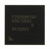
Manufacturer Part Number
DF2506BR26DV
Description
IC H8S/2506 MCU FLASH 176-LFBGA
Manufacturer
Renesas Electronics America
Series
H8® H8S/2500r
Specifications of DF2506BR26DV
Core Processor
H8S/2000
Core Size
16-Bit
Speed
26MHz
Connectivity
I²C, SCI
Peripherals
POR, PWM, WDT
Number Of I /o
104
Program Memory Size
512KB (512K x 8)
Program Memory Type
FLASH
Ram Size
32K x 8
Voltage - Supply (vcc/vdd)
3 V ~ 5.5 V
Data Converters
A/D 16x10b; D/A 2x8b
Oscillator Type
Internal
Operating Temperature
-40°C ~ 85°C
Package / Case
176-LFBGA
Lead Free Status / RoHS Status
Lead free / RoHS Compliant
Eeprom Size
-
Available stocks
Company
Part Number
Manufacturer
Quantity
Price
Company:

Part Number:
DF2506BR26DV
Manufacturer:
Renesas Electronics America
Quantity:
10 000


Table 10.7
Table 10.8
Table 10.9
Table 10.10 TPSC0 to TPSC2 (channel 5).................................................................................. 280
Table 10.11 MD0 to MD3........................................................................................................... 282
Table 10.12 TIORH_0 ................................................................................................................ 284
Table 10.13 TIORL_0 ................................................................................................................. 285
Table 10.14 TIOR_1 ................................................................................................................... 286
Table 10.15 TIOR_2 ................................................................................................................... 287
Table 10.16 TIORH_3 ................................................................................................................ 288
Table 10.17 TIORL_3 ................................................................................................................. 289
Table 10.18 TIOR_4 ................................................................................................................... 290
Table 10.19 TIOR_5 ................................................................................................................... 291
Table 10.20 TIORH_0 ................................................................................................................ 292
Table 10.21 TIORL_0 ................................................................................................................. 293
Table 10.22 TIOR_1 ................................................................................................................... 294
Table 10.23 TIOR_2 ................................................................................................................... 295
Table 10.24 TIORH_3 ................................................................................................................ 296
Table 10.25 TIORL_3 ................................................................................................................. 297
Table 10.26 TIOR_4 ................................................................................................................... 298
Table 10.27 TIOR_5 ................................................................................................................... 299
Table 10.28 Register Combinations in Buffer Operation............................................................ 315
Table 10.29 Cascaded Combinations .......................................................................................... 318
Table 10.30 PWM Output Registers and Output Pins................................................................. 321
Table 10.31 Phase Counting Mode Clock Input Pins.................................................................. 325
Table 10.32 Up/Down-Count Conditions in Phase Counting Mode 1 ........................................ 327
Table 10.33 Up/Down-Count Conditions in Phase Counting Mode 2 ........................................ 328
Table 10.34 Up/Down-Count Conditions in Phase Counting Mode 3 ........................................ 329
Table 10.35 Up/Down-Count Conditions in Phase Counting Mode 4 ........................................ 330
Table 10.36 TPU Interrupts......................................................................................................... 333
Section 11 8-Bit Timers (TMR)
Table 11.1
Table 11.2
Table 11.3
Table 11.4
Section 12 Watchdog Timer (WDT)
Table 12.1
Table 12.2
TPSC0 to TPSC2 (channels 2) ................................................................................ 279
TPSC0 to TPSC2 (channel 3).................................................................................. 279
TPSC0 to TPSC2 (channel 4).................................................................................. 280
Pin Configuration .................................................................................................... 355
8-Bit Timer Interrupt Sources ................................................................................. 370
Timer Output Priorities ........................................................................................... 373
Switching of Internal Clock and TCNT Operation ................................................. 374
Pin Configuration .................................................................................................... 379
WDT Interrupt Source............................................................................................. 389
Rev. 6.00 Sep. 24, 2009 Page xliii of xlvi
REJ09B0099-0600
Related parts for DF2506BR26DV
Image
Part Number
Description
Manufacturer
Datasheet
Request
R

Part Number:
Description:
KIT STARTER FOR M16C/29
Manufacturer:
Renesas Electronics America
Datasheet:

Part Number:
Description:
KIT STARTER FOR R8C/2D
Manufacturer:
Renesas Electronics America
Datasheet:

Part Number:
Description:
R0K33062P STARTER KIT
Manufacturer:
Renesas Electronics America
Datasheet:

Part Number:
Description:
KIT STARTER FOR R8C/23 E8A
Manufacturer:
Renesas Electronics America
Datasheet:

Part Number:
Description:
KIT STARTER FOR R8C/25
Manufacturer:
Renesas Electronics America
Datasheet:

Part Number:
Description:
KIT STARTER H8S2456 SHARPE DSPLY
Manufacturer:
Renesas Electronics America
Datasheet:

Part Number:
Description:
KIT STARTER FOR R8C38C
Manufacturer:
Renesas Electronics America
Datasheet:

Part Number:
Description:
KIT STARTER FOR R8C35C
Manufacturer:
Renesas Electronics America
Datasheet:

Part Number:
Description:
KIT STARTER FOR R8CL3AC+LCD APPS
Manufacturer:
Renesas Electronics America
Datasheet:
Part Number:
Description:
KIT STARTER FOR RX610
Manufacturer:
Renesas Electronics America
Datasheet:

Part Number:
Description:
KIT STARTER FOR R32C/118
Manufacturer:
Renesas Electronics America
Datasheet:

Part Number:
Description:
KIT DEV RSK-R8C/26-29
Manufacturer:
Renesas Electronics America
Datasheet:

Part Number:
Description:
KIT STARTER FOR SH7124
Manufacturer:
Renesas Electronics America
Datasheet:

Part Number:
Description:
KIT STARTER FOR H8SX/1622
Manufacturer:
Renesas Electronics America
Datasheet:

Part Number:
Description:
KIT DEV FOR SH7203
Manufacturer:
Renesas Electronics America
Datasheet: