AT91SAM9R64-CU Atmel, AT91SAM9R64-CU Datasheet - Page 71
AT91SAM9R64-CU
Manufacturer Part Number
AT91SAM9R64-CU
Description
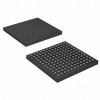
MCU ARM9 64K SRAM 144-LFBGA
Manufacturer
Atmel
Series
AT91SAMr
Specifications of AT91SAM9R64-CU
Core Processor
ARM9
Core Size
16/32-Bit
Speed
240MHz
Connectivity
EBI/EMI, I²C, MMC, SPI, SSC, UART/USART, USB
Peripherals
AC'97, POR, PWM, WDT
Number Of I /o
49
Program Memory Size
32KB (32K x 8)
Program Memory Type
ROM
Ram Size
72K x 8
Voltage - Supply (vcc/vdd)
1.08 V ~ 1.32 V
Data Converters
A/D 3x10b
Oscillator Type
Internal
Operating Temperature
-40°C ~ 85°C
Package / Case
144-LFBGA
Processor Series
AT91SAMx
Core
ARM926EJ-S
Data Bus Width
32 bit
Data Ram Size
64 KB
Interface Type
2-Wire, SPI, SSC, USART
Maximum Clock Frequency
240 MHz
Number Of Programmable I/os
118
Number Of Timers
4
Maximum Operating Temperature
+ 85 C
Mounting Style
SMD/SMT
3rd Party Development Tools
JTRACE-ARM-2M, MDK-ARM, RL-ARM, ULINK2
Development Tools By Supplier
AT91SAM-ICE, AT91-ISP, AT91SAM9RL-EK
Minimum Operating Temperature
- 40 C
On-chip Adc
10 bit, 3 Channel
Controller Family/series
AT91SAM9xxx
No. Of I/o's
49
Ram Memory Size
64KB
Cpu Speed
240MHz
No. Of Timers
3
Rohs Compliant
Yes
Package
144LFBGA
Device Core
ARM926EJ-S
Family Name
91S
Maximum Speed
240 MHz
Operating Supply Voltage
1.8|3.3 V
For Use With
AT91SAM-ICE - EMULATOR FOR AT91 ARM7/ARM9
Lead Free Status / RoHS Status
Lead free / RoHS Compliant
Eeprom Size
-
Lead Free Status / Rohs Status
Lead free / RoHS Compliant
Available stocks
Company
Part Number
Manufacturer
Quantity
Price

Part Number:
AT91SAM9R64-CU
Manufacturer:
ATMEL/爱特梅尔
Quantity:
20 000


13.5.3
13.5.4
13.5.5
6289C–ATARM–28-May-09
JTAG Signal Description
Debug Unit
IEEE 1149.1 JTAG Boundary Scan
TMS is the Test Mode Select input which controls the transitions of the test interface state
machine.
TDI is the Test Data Input line which supplies the data to the JTAG registers (Boundary Scan
Register, Instruction Register, or other data registers).
TDO is the Test Data Output line which is used to serially output the data from the JTAG regis-
ters to the equipment controlling the test. It carries the sampled values from the boundary scan
chain (or other JTAG registers) and propagates them to the next chip in the serial test circuit.
NTRST (optional in IEEE Standard 1149.1) is a Test-ReSeT input which is mandatory in ARM
cores and used to reset the debug logic. On Atmel ARM926EJ-S-based cores, NTRST is a
Power On Reset output. It is asserted on power on. If necessary, the user can also reset the
debug logic with the NTRST pin assertion during 2.5 MCK periods.
TCK is the Test ClocK input which enables the test interface. TCK is pulsed by the equipment
controlling the test and not by the tested device. It can be pulsed at any frequency. Note the
maximum JTAG clock rate on ARM926EJ-S cores is 1/6th the clock of the CPU. This gives 5.45
kHz maximum initial JTAG clock rate for an ARM9E running from the 32.768 kHz slow clock.
RTCK is the Return Test Clock. Not an IEEE Standard 1149.1 signal added for a better clock
handling by emulators. From some ICE Interface probes, this return signal can be used to syn-
chronize the TCK clock and take not care about the given ratio between the ICE Interface clock
and system clock equal to 1/6th. This signal is only available in JTAG ICE Mode and not in
boundary scan mode.
The Debug Unit provides a two-pin (DXRD and TXRD) USART that can be used for several
debug and trace purposes and offers an ideal means for in-situ programming solutions and
debug monitor communication. Moreover, the association with two peripheral data controller
channels permits packet handling of these tasks with processor time reduced to a minimum.
The Debug Unit also manages the interrupt handling of the COMMTX and COMMRX signals
that come from the ICE and that trace the activity of the Debug Communication Channel.The
Debug Unit allows blockage of access to the system through the ICE interface.
A specific register, the Debug Unit Chip ID Register, gives information about the product version
and its internal configuration.
The AT91SAM9R64/RL64 Debug Unit Chip ID value is 0x0196 07A0 on 32-bit width.
For further details on the Debug Unit, see the Debug Unit section.
IEEE 1149.1 JTAG Boundary Scan allows pin-level access independent of the device packaging
technology.
IEEE 1149.1 JTAG Boundary Scan is enabled when JTAGSEL is high. The SAMPLE, EXTEST
and BYPASS functions are implemented. In ICE debug mode, the ARM processor responds
with a non-JTAG chip ID that identifies the processor to the ICE system. This is not IEEE 1149.1
JTAG-compliant.
It is not possible to switch directly between JTAG and ICE operations. A chip reset must be per-
formed after JTAGSEL is changed.
AT91SAM9R64/RL64 Preliminary
71
Related parts for AT91SAM9R64-CU
Image
Part Number
Description
Manufacturer
Datasheet
Request
R

Part Number:
Description:
MCU, MPU & DSP Development Tools KICKSTART KIT FOR AT91SAM9 PLUS
Manufacturer:
IAR Systems

Part Number:
Description:
DEV KIT FOR AVR/AVR32
Manufacturer:
Atmel
Datasheet:

Part Number:
Description:
INTERVAL AND WIPE/WASH WIPER CONTROL IC WITH DELAY
Manufacturer:
ATMEL Corporation
Datasheet:
Part Number:
Description:
Low-Voltage Voice-Switched IC for Hands-Free Operation
Manufacturer:
ATMEL Corporation
Datasheet:
Part Number:
Description:
MONOLITHIC INTEGRATED FEATUREPHONE CIRCUIT
Manufacturer:
ATMEL Corporation
Datasheet:
Part Number:
Description:
AM-FM Receiver IC U4255BM-M
Manufacturer:
ATMEL Corporation
Datasheet:
Part Number:
Description:
Monolithic Integrated Feature Phone Circuit
Manufacturer:
ATMEL Corporation
Datasheet:
Part Number:
Description:
Multistandard Video-IF and Quasi Parallel Sound Processing
Manufacturer:
ATMEL Corporation
Datasheet:
Part Number:
Description:
High-performance EE PLD
Manufacturer:
ATMEL Corporation
Datasheet:
Part Number:
Description:
8-bit Flash Microcontroller
Manufacturer:
ATMEL Corporation
Datasheet:
Part Number:
Description:
2-Wire Serial EEPROM
Manufacturer:
ATMEL Corporation
Datasheet: