AT91SAM9R64-CU Atmel, AT91SAM9R64-CU Datasheet - Page 666
AT91SAM9R64-CU
Manufacturer Part Number
AT91SAM9R64-CU
Description
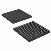
MCU ARM9 64K SRAM 144-LFBGA
Manufacturer
Atmel
Series
AT91SAMr
Specifications of AT91SAM9R64-CU
Core Processor
ARM9
Core Size
16/32-Bit
Speed
240MHz
Connectivity
EBI/EMI, I²C, MMC, SPI, SSC, UART/USART, USB
Peripherals
AC'97, POR, PWM, WDT
Number Of I /o
49
Program Memory Size
32KB (32K x 8)
Program Memory Type
ROM
Ram Size
72K x 8
Voltage - Supply (vcc/vdd)
1.08 V ~ 1.32 V
Data Converters
A/D 3x10b
Oscillator Type
Internal
Operating Temperature
-40°C ~ 85°C
Package / Case
144-LFBGA
Processor Series
AT91SAMx
Core
ARM926EJ-S
Data Bus Width
32 bit
Data Ram Size
64 KB
Interface Type
2-Wire, SPI, SSC, USART
Maximum Clock Frequency
240 MHz
Number Of Programmable I/os
118
Number Of Timers
4
Maximum Operating Temperature
+ 85 C
Mounting Style
SMD/SMT
3rd Party Development Tools
JTRACE-ARM-2M, MDK-ARM, RL-ARM, ULINK2
Development Tools By Supplier
AT91SAM-ICE, AT91-ISP, AT91SAM9RL-EK
Minimum Operating Temperature
- 40 C
On-chip Adc
10 bit, 3 Channel
Controller Family/series
AT91SAM9xxx
No. Of I/o's
49
Ram Memory Size
64KB
Cpu Speed
240MHz
No. Of Timers
3
Rohs Compliant
Yes
Package
144LFBGA
Device Core
ARM926EJ-S
Family Name
91S
Maximum Speed
240 MHz
Operating Supply Voltage
1.8|3.3 V
For Use With
AT91SAM-ICE - EMULATOR FOR AT91 ARM7/ARM9
Lead Free Status / RoHS Status
Lead free / RoHS Compliant
Eeprom Size
-
Lead Free Status / Rohs Status
Lead free / RoHS Compliant
Available stocks
Company
Part Number
Manufacturer
Quantity
Price

Part Number:
AT91SAM9R64-CU
Manufacturer:
ATMEL/爱特梅尔
Quantity:
20 000


output brings the value of the polarity (POL) bit in the PWM control register: CONTRAST_CTR.
Otherwise, the opposite value is output. Thus, a periodic waveform with a pulse width propor-
tional to the value in the compare register is generated.
Due to the comparison mechanism, the output pulse has a width between zero and 255 PWM
counter cycles. Thus by adding a simple passive filter outside the chip, an analog voltage
between 0 and (255/256) × VDD can be obtained (for the positive polarity case, or between
(1/256) × VDD and VDD for the negative polarity case). Other voltage values can be obtained by
adding active external circuitry.
For PWM mode, the frequency of the counter can be adjusted to four different values using field
PS of CONTRAST_CTR register.
39.5.3
LCD Interface
The LCD Controller interfaces with the LCD Module through the LCD Interface
(Table 39-12 on
page
671). The Controller supports the following interface configurations: 24-bit TFT single
scan, 16-bit STN Dual Scan Mono (Color), 8-bit STN Dual (Single) Scan Mono (Color), 4-bit sin-
gle scan Mono (Color).
A 4-bit single scan STN display uses 4 parallel data lines to shift data to successive single hori-
zontal lines one at a time until the entire frame has been shifted and transferred. The 4 LSB pins
of LCD Data Bus (LCDD [3:0]) can be directly connected to the LCD driver; the 20 MSB pins
(LCDD [23:4]) are not used.
An 8-bit single scan STN display uses 8 parallel data lines to shift data to successive single hor-
izontal lines one at a time until the entire frame has been shifted and transferred. The 8 LSB pins
of LCD Data Bus (LCDD [7:0]) can be directly connected to the LCD driver; the 16 MSB pins
(LCDD [23:8]) are not used.
An 8-bit Dual Scan STN display uses two sets of 4 parallel data lines to shift data to successive
upper and lower panel horizontal lines one at a time until the entire frame has been shifted and
transferred. The bus LCDD[3:0] is connected to the upper panel data lines and the bus
LCDD[7:4] is connected to the lower panel data lines. The rest of the LCD Data Bus lines
(LCDD[23:8]) are not used.
A 16-bit Dual Scan STN display uses two sets of 8 parallel data lines to shift data to successive
upper and lower panel horizontal lines one at a time until the entire frame has been shifted and
transferred. The bus LCDD[7:0] is connected to the upper panel data lines and the bus
LCDD[15:8] is connected to the lower panel data lines. The rest of the LCD Data Bus lines
(LCDD[23:16]) are not used.
STN Mono displays require one bit of image data per pixel. STN Color displays require three bits
(Red, Green and Blue) of image data per pixel, resulting in a horizontal shift register of length
three times the number of pixels per horizontal line. This RGB or Monochrome data is shifted to
the LCD driver as consecutive bits via the parallel data lines.
A TFT single scan display uses up to 24 parallel data lines to shift data to successive horizontal
lines one at a time until the entire frame has been shifted and transferred. The 24 data lines are
divided in three bytes that define the color shade of each color component of each pixel. The
LCDD bus is split as LCDD[23:16] for the blue component, LCDD[15:8] for the green component
and LCDD[7:0] for the red component. If the LCD Module has lower color resolution (fewer bits
per color component), only the most significant bits of each component are used.
AT91SAM9R64/RL64 Preliminary
666
6289C–ATARM–28-May-09
Related parts for AT91SAM9R64-CU
Image
Part Number
Description
Manufacturer
Datasheet
Request
R

Part Number:
Description:
MCU, MPU & DSP Development Tools KICKSTART KIT FOR AT91SAM9 PLUS
Manufacturer:
IAR Systems

Part Number:
Description:
DEV KIT FOR AVR/AVR32
Manufacturer:
Atmel
Datasheet:

Part Number:
Description:
INTERVAL AND WIPE/WASH WIPER CONTROL IC WITH DELAY
Manufacturer:
ATMEL Corporation
Datasheet:
Part Number:
Description:
Low-Voltage Voice-Switched IC for Hands-Free Operation
Manufacturer:
ATMEL Corporation
Datasheet:
Part Number:
Description:
MONOLITHIC INTEGRATED FEATUREPHONE CIRCUIT
Manufacturer:
ATMEL Corporation
Datasheet:
Part Number:
Description:
AM-FM Receiver IC U4255BM-M
Manufacturer:
ATMEL Corporation
Datasheet:
Part Number:
Description:
Monolithic Integrated Feature Phone Circuit
Manufacturer:
ATMEL Corporation
Datasheet:
Part Number:
Description:
Multistandard Video-IF and Quasi Parallel Sound Processing
Manufacturer:
ATMEL Corporation
Datasheet:
Part Number:
Description:
High-performance EE PLD
Manufacturer:
ATMEL Corporation
Datasheet:
Part Number:
Description:
8-bit Flash Microcontroller
Manufacturer:
ATMEL Corporation
Datasheet:
Part Number:
Description:
2-Wire Serial EEPROM
Manufacturer:
ATMEL Corporation
Datasheet: