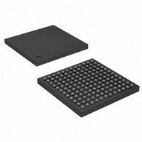
AT91SAM9R64-CU Atmel, AT91SAM9R64-CU Datasheet - Page 353

AT91SAM9R64-CU
Manufacturer Part Number
AT91SAM9R64-CU
Description
MCU ARM9 64K SRAM 144-LFBGA
Manufacturer
Atmel
Series
AT91SAMr
Specifications of AT91SAM9R64-CU
Core Processor
ARM9
Core Size
16/32-Bit
Speed
240MHz
Connectivity
EBI/EMI, I²C, MMC, SPI, SSC, UART/USART, USB
Peripherals
AC'97, POR, PWM, WDT
Number Of I /o
49
Program Memory Size
32KB (32K x 8)
Program Memory Type
ROM
Ram Size
72K x 8
Voltage - Supply (vcc/vdd)
1.08 V ~ 1.32 V
Data Converters
A/D 3x10b
Oscillator Type
Internal
Operating Temperature
-40°C ~ 85°C
Package / Case
144-LFBGA
Processor Series
AT91SAMx
Core
ARM926EJ-S
Data Bus Width
32 bit
Data Ram Size
64 KB
Interface Type
2-Wire, SPI, SSC, USART
Maximum Clock Frequency
240 MHz
Number Of Programmable I/os
118
Number Of Timers
4
Maximum Operating Temperature
+ 85 C
Mounting Style
SMD/SMT
3rd Party Development Tools
JTRACE-ARM-2M, MDK-ARM, RL-ARM, ULINK2
Development Tools By Supplier
AT91SAM-ICE, AT91-ISP, AT91SAM9RL-EK
Minimum Operating Temperature
- 40 C
On-chip Adc
10 bit, 3 Channel
Controller Family/series
AT91SAM9xxx
No. Of I/o's
49
Ram Memory Size
64KB
Cpu Speed
240MHz
No. Of Timers
3
Rohs Compliant
Yes
Package
144LFBGA
Device Core
ARM926EJ-S
Family Name
91S
Maximum Speed
240 MHz
Operating Supply Voltage
1.8|3.3 V
For Use With
AT91SAM-ICE - EMULATOR FOR AT91 ARM7/ARM9
Lead Free Status / RoHS Status
Lead free / RoHS Compliant
Eeprom Size
-
Lead Free Status / Rohs Status
Lead free / RoHS Compliant
Available stocks
Company
Part Number
Manufacturer
Quantity
Price
Part Number:
AT91SAM9R64-CU
Manufacturer:
ATMEL/爱特梅尔
Quantity:
20 000
- Current page: 353 of 903
- Download datasheet (13Mb)
Figure 31-4. Output Line Timings
31.4.8
31.4.9
6289C–ATARM–28-May-09
Write PIO_ODSR at 1
Write PIO_ODSR at 0
Write PIO_CODR
Write PIO_SODR
Inputs
Input Glitch Filtering
PIO_ODSR
PIO_PDSR
MCK
The level on each I/O line can be read through PIO_PDSR (Pin Data Status Register). This reg-
ister indicates the level of the I/O lines regardless of their configuration, whether uniquely as an
input or driven by the PIO controller or driven by a peripheral.
Reading the I/O line levels requires the clock of the PIO controller to be enabled, otherwise
PIO_PDSR reads the levels present on the I/O line at the time the clock was disabled.
Optional input glitch filters are independently programmable on each I/O line. When the glitch fil-
ter is enabled, a glitch with a duration of less than 1/2 Master Clock (MCK) cycle is automatically
rejected, while a pulse with a duration of 1 Master Clock cycle or more is accepted. For pulse
durations between 1/2 Master Clock cycle and 1 Master Clock cycle the pulse may or may not
be taken into account, depending on the precise timing of its occurrence. Thus for a pulse to be
visible it must exceed 1 Master Clock cycle, whereas for a glitch to be reliably filtered out, its
duration must not exceed 1/2 Master Clock cycle. The filter introduces one Master Clock cycle
latency if the pin level change occurs before a rising edge. However, this latency does not
appear if the pin level change occurs before a falling edge. This is illustrated in
The glitch filters are controlled by the register set; PIO_IFER (Input Filter Enable Register),
PIO_IFDR (Input Filter Disable Register) and PIO_IFSR (Input Filter Status Register). Writing
PIO_IFER and PIO_IFDR respectively sets and clears bits in PIO_IFSR. This last register
enables the glitch filter on the I/O lines.
When the glitch filter is enabled, it does not modify the behavior of the inputs on the peripherals.
It acts only on the value read in PIO_PDSR and on the input change interrupt detection. The
glitch filters require that the PIO Controller clock is enabled.
APB Access
2 cycles
AT91SAM9R64/RL64 Preliminary
APB Access
2 cycles
Figure
31-5.
353
Related parts for AT91SAM9R64-CU
Image
Part Number
Description
Manufacturer
Datasheet
Request
R

Part Number:
Description:
MCU, MPU & DSP Development Tools KICKSTART KIT FOR AT91SAM9 PLUS
Manufacturer:
IAR Systems

Part Number:
Description:
DEV KIT FOR AVR/AVR32
Manufacturer:
Atmel
Datasheet:

Part Number:
Description:
INTERVAL AND WIPE/WASH WIPER CONTROL IC WITH DELAY
Manufacturer:
ATMEL Corporation
Datasheet:

Part Number:
Description:
Low-Voltage Voice-Switched IC for Hands-Free Operation
Manufacturer:
ATMEL Corporation
Datasheet:

Part Number:
Description:
MONOLITHIC INTEGRATED FEATUREPHONE CIRCUIT
Manufacturer:
ATMEL Corporation
Datasheet:

Part Number:
Description:
AM-FM Receiver IC U4255BM-M
Manufacturer:
ATMEL Corporation
Datasheet:

Part Number:
Description:
Monolithic Integrated Feature Phone Circuit
Manufacturer:
ATMEL Corporation
Datasheet:

Part Number:
Description:
Multistandard Video-IF and Quasi Parallel Sound Processing
Manufacturer:
ATMEL Corporation
Datasheet:

Part Number:
Description:
High-performance EE PLD
Manufacturer:
ATMEL Corporation
Datasheet:

Part Number:
Description:
8-bit Flash Microcontroller
Manufacturer:
ATMEL Corporation
Datasheet:

Part Number:
Description:
2-Wire Serial EEPROM
Manufacturer:
ATMEL Corporation
Datasheet:


