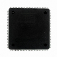
AT32AP7001-ALUT Atmel, AT32AP7001-ALUT Datasheet - Page 746

AT32AP7001-ALUT
Manufacturer Part Number
AT32AP7001-ALUT
Description
IC MCU 32BIT AVR32 208-LQFP
Manufacturer
Atmel
Series
AVR®32 AP7r
Specifications of AT32AP7001-ALUT
Core Processor
AVR
Core Size
32-Bit
Speed
150MHz
Connectivity
EBI/EMI, I²C, MMC, PS2, SPI, SSC, UART/USART, USB
Peripherals
AC'97, DMA, I²C, POR, PWM, WDT
Number Of I /o
90
Program Memory Type
ROMless
Ram Size
32K x 8
Voltage - Supply (vcc/vdd)
1.65 V ~ 1.95 V
Data Converters
D/A 2x16b
Oscillator Type
Internal
Operating Temperature
-40°C ~ 85°C
Package / Case
208-LQFP
Data Bus Width
32 bit
Data Ram Size
32 KB
Interface Type
EBI, ISI, MCI, PS2, SPI, TWI, USB
Maximum Clock Frequency
150 MHz
Number Of Programmable I/os
90
Number Of Timers
3
Maximum Operating Temperature
+ 85 C
Mounting Style
SMD/SMT
Minimum Operating Temperature
- 40 C
On-chip Dac
16 bit, 1 Channel
Package
208PQFP
Device Core
AVR32
Family Name
AT32
Maximum Speed
150 MHz
Operating Supply Voltage
1.8 V
For Use With
ATAVRONEKIT - KIT AVR/AVR32 DEBUGGER/PROGRMMRATNGW100 - KIT AVR32 NETWORK GATEWAYATSTK1000 - KIT STARTER FOR AVR32AP7000
Lead Free Status / RoHS Status
Lead free / RoHS Compliant
Eeprom Size
-
Program Memory Size
-
Lead Free Status / Rohs Status
Details
Available stocks
Company
Part Number
Manufacturer
Quantity
Price
Company:
Part Number:
AT32AP7001-ALUT
Manufacturer:
EVERLIGHT
Quantity:
12 000
- Current page: 746 of 829
- Download datasheet (12Mb)
35.5.4.3
35.5.4.4
35.5.4.5
32015G–AVR32–09/09
Memory Interface
FIFO and DMA Features
Example
Preview datapath contains a data formatter that converts 8:8:8 pixel to RGB 5:5:5 format. In
general, when converting from a color channel with more bits to one with fewer bits, formatter
module discards the lower-order bits. Example: Converting from RGB 8:8:8 to RGB 5:6:5, it dis-
cards the three LSBs from the red and blue channels, and two LSBs from the green channel.
When grayscale mode is enabled, two memory format are supported. One mode supports 2 pix-
els per word, and the other mode supports 1 pixel per word.
Table 35-8.
Both preview and Codec datapaths contain FIFOs, asynchronous buffers that are used to safely
transfer formatted pixels from Pixel clock domain to High Speed Bus (HSB) clock domain. A
video arbiter is used to manage FIFO thresholds and triggers a relevant DMA request through
the HSB master interface. Thus, depending on FIFO state, a specified length burst is asserted.
Regarding HSB master interface, it supports Scatter DMA mode through linked list operation.
This mode of operation improves flexibility of image buffer location and allows the user to allo-
cate two or more frame buffers. The destination frame buffers are defined by a series of Frame
Buffer Descriptors (FBD). Each FBD controls the transfer of one entire frame and then optionally
loads a further FBD to switch the DMA operation at another frame buffer address. The FBD is
defined by a series of two words. The first one defines the current frame buffer address, and the
second defines the next FBD memory location. This DMA transfer mode is only available for pre-
view datapath and is configured in the PPFBD register that indicates the memory location of the
first FBD.
The primary FBD is programmed into the camera interface controller. The data to be transferred
described by an FBD requires several burst access. In the example below, the use of 2 ping-
pong frame buffers is described.
The first FBD, stored at address 0x30000, defines the location of the first frame buffer.
Destination Address: frame buffer ID0 0x02A000
Next FBD address: 0x30010
Second FBD, stored at address 0x30010, defines the location of the second frame buffer.
Destination Address: frame buffer ID1 0x3A000
Transfer width: 32 bit
Next FBD address: 0x30000, wrapping to first FBD.
Using this technique, several frame buffers can be configured through the linked list.
illustrates a typical three frame buffer application. Frame n is mapped to frame buffer 0, frame
n+1 is mapped to frame buffer 1, frame n+2 is mapped to Frame buffer 2, further frames wrap. A
codec request occurs, and the full-size 4:2:2 encoded frame is stored in a dedicated memory
space.
GS_MODE
0
1
Grayscale Memory Mapping Configuration for 12-bit Data
DATA[31:24]
P_0[11:4]
P_0[11:4]
DATA[23:16]
P_0[3:0], 0000
P_0[3:0], 0000
DATA[15:8]
P_1[11:4]
0
AT32AP7001
DATA[7:0]
P_1[3:0], 0000
0
Figure 35-6
746
Related parts for AT32AP7001-ALUT
Image
Part Number
Description
Manufacturer
Datasheet
Request
R

Part Number:
Description:
DEV KIT FOR AVR/AVR32
Manufacturer:
Atmel
Datasheet:

Part Number:
Description:
INTERVAL AND WIPE/WASH WIPER CONTROL IC WITH DELAY
Manufacturer:
ATMEL Corporation
Datasheet:

Part Number:
Description:
Low-Voltage Voice-Switched IC for Hands-Free Operation
Manufacturer:
ATMEL Corporation
Datasheet:

Part Number:
Description:
MONOLITHIC INTEGRATED FEATUREPHONE CIRCUIT
Manufacturer:
ATMEL Corporation
Datasheet:

Part Number:
Description:
AM-FM Receiver IC U4255BM-M
Manufacturer:
ATMEL Corporation
Datasheet:

Part Number:
Description:
Monolithic Integrated Feature Phone Circuit
Manufacturer:
ATMEL Corporation
Datasheet:

Part Number:
Description:
Multistandard Video-IF and Quasi Parallel Sound Processing
Manufacturer:
ATMEL Corporation
Datasheet:

Part Number:
Description:
High-performance EE PLD
Manufacturer:
ATMEL Corporation
Datasheet:

Part Number:
Description:
8-bit Flash Microcontroller
Manufacturer:
ATMEL Corporation
Datasheet:

Part Number:
Description:
2-Wire Serial EEPROM
Manufacturer:
ATMEL Corporation
Datasheet:


