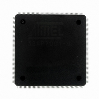
AT32AP7001-ALUT Atmel, AT32AP7001-ALUT Datasheet - Page 254

AT32AP7001-ALUT
Manufacturer Part Number
AT32AP7001-ALUT
Description
IC MCU 32BIT AVR32 208-LQFP
Manufacturer
Atmel
Series
AVR®32 AP7r
Specifications of AT32AP7001-ALUT
Core Processor
AVR
Core Size
32-Bit
Speed
150MHz
Connectivity
EBI/EMI, I²C, MMC, PS2, SPI, SSC, UART/USART, USB
Peripherals
AC'97, DMA, I²C, POR, PWM, WDT
Number Of I /o
90
Program Memory Type
ROMless
Ram Size
32K x 8
Voltage - Supply (vcc/vdd)
1.65 V ~ 1.95 V
Data Converters
D/A 2x16b
Oscillator Type
Internal
Operating Temperature
-40°C ~ 85°C
Package / Case
208-LQFP
Data Bus Width
32 bit
Data Ram Size
32 KB
Interface Type
EBI, ISI, MCI, PS2, SPI, TWI, USB
Maximum Clock Frequency
150 MHz
Number Of Programmable I/os
90
Number Of Timers
3
Maximum Operating Temperature
+ 85 C
Mounting Style
SMD/SMT
Minimum Operating Temperature
- 40 C
On-chip Dac
16 bit, 1 Channel
Package
208PQFP
Device Core
AVR32
Family Name
AT32
Maximum Speed
150 MHz
Operating Supply Voltage
1.8 V
For Use With
ATAVRONEKIT - KIT AVR/AVR32 DEBUGGER/PROGRMMRATNGW100 - KIT AVR32 NETWORK GATEWAYATSTK1000 - KIT STARTER FOR AVR32AP7000
Lead Free Status / RoHS Status
Lead free / RoHS Compliant
Eeprom Size
-
Program Memory Size
-
Lead Free Status / Rohs Status
Details
Available stocks
Company
Part Number
Manufacturer
Quantity
Price
Company:
Part Number:
AT32AP7001-ALUT
Manufacturer:
EVERLIGHT
Quantity:
12 000
- Current page: 254 of 829
- Download datasheet (12Mb)
20.5.5
20.5.6
20.5.7
Figure 20-4. Output Line Timings
32015G–AVR32–09/09
Write ODSR at 1
Write ODSR at 0
Multi-drive capability
Synchronous Data Output
Output Line Timings
Write CODR
Write SODR
CLK_PIO
ODSR
PDSR
register is at 0, the corresponding I/O line is used as an input only. When the bit is at 1, the cor-
responding I/O line is driven by the PIO controller.
The level driven on an I/O line can be determined by writing in SODR (Set Output Data Register)
and CODR (Clear Output Data Register). These write operations respectively set and clear
ODSR (Output Data Status Register), which represents the data driven on the I/O lines. Writing
in OER and ODR manages OSR whether the pin is configured to be controlled by the PIO con-
troller or assigned to a peripheral function. This enables configuration of the I/O line prior to
setting it to be managed by the PIO Controller.
Similarly, writing in SODR and CODR effects ODSR. This is important as it defines the first level
driven on the I/O line.
The PIO is able to configure each pin as open drain to support external drivers on the same pin.
This is done by writing MDER (Multi-Drive Enable Register) and MDDR (Multi-Drive Disable
Register). The result of these write operations are detected in MDSR (multui-Drive Status Regis-
ter). The multi-drive mode is only available when the PIO is controlling the pin, i.e. PSR is set.
When using multi-drive the PIO will tri-state the pin when ODSR is set and drive the pin low
when ODSR is cleared. writing to OER or ODR will have no effect.
Controlling all parallel busses using several PIOs requires two successive write operations in the
SODR and CODR registers. This may lead to unexpected transient values. The PIO controller
offers a direct control of PIO outputs by single write access to ODSR (Output Data Status Regis-
ter). Only bits unmasked by OWSR (Output Write Status Register) are written. The mask bits in
the OWSR are set by writing to OWER (Output Write Enable Register) and cleared by writing to
OWDR (Output Write Disable Register).
After reset, the synchronous data output is disabled on all the I/O lines as OWSR resets at 0x0.
Figure 20-4
writing ODSR. This last case is valid only if the corresponding bit in OWSR is set.
also shows when the feedback in PDSR is available.
Peripheral Bus Access
shows how the outputs are driven either by writing SODR or CODR, or by directly
2 cycles
Peripheral Bus Access
AT32AP7001
2 cycles
Figure 20-4
254
Related parts for AT32AP7001-ALUT
Image
Part Number
Description
Manufacturer
Datasheet
Request
R

Part Number:
Description:
DEV KIT FOR AVR/AVR32
Manufacturer:
Atmel
Datasheet:

Part Number:
Description:
INTERVAL AND WIPE/WASH WIPER CONTROL IC WITH DELAY
Manufacturer:
ATMEL Corporation
Datasheet:

Part Number:
Description:
Low-Voltage Voice-Switched IC for Hands-Free Operation
Manufacturer:
ATMEL Corporation
Datasheet:

Part Number:
Description:
MONOLITHIC INTEGRATED FEATUREPHONE CIRCUIT
Manufacturer:
ATMEL Corporation
Datasheet:

Part Number:
Description:
AM-FM Receiver IC U4255BM-M
Manufacturer:
ATMEL Corporation
Datasheet:

Part Number:
Description:
Monolithic Integrated Feature Phone Circuit
Manufacturer:
ATMEL Corporation
Datasheet:

Part Number:
Description:
Multistandard Video-IF and Quasi Parallel Sound Processing
Manufacturer:
ATMEL Corporation
Datasheet:

Part Number:
Description:
High-performance EE PLD
Manufacturer:
ATMEL Corporation
Datasheet:

Part Number:
Description:
8-bit Flash Microcontroller
Manufacturer:
ATMEL Corporation
Datasheet:

Part Number:
Description:
2-Wire Serial EEPROM
Manufacturer:
ATMEL Corporation
Datasheet:


