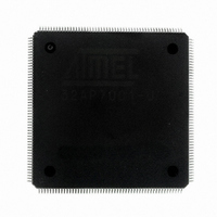
AT32AP7001-ALUT Atmel, AT32AP7001-ALUT Datasheet - Page 495

AT32AP7001-ALUT
Manufacturer Part Number
AT32AP7001-ALUT
Description
IC MCU 32BIT AVR32 208-LQFP
Manufacturer
Atmel
Series
AVR®32 AP7r
Specifications of AT32AP7001-ALUT
Core Processor
AVR
Core Size
32-Bit
Speed
150MHz
Connectivity
EBI/EMI, I²C, MMC, PS2, SPI, SSC, UART/USART, USB
Peripherals
AC'97, DMA, I²C, POR, PWM, WDT
Number Of I /o
90
Program Memory Type
ROMless
Ram Size
32K x 8
Voltage - Supply (vcc/vdd)
1.65 V ~ 1.95 V
Data Converters
D/A 2x16b
Oscillator Type
Internal
Operating Temperature
-40°C ~ 85°C
Package / Case
208-LQFP
Data Bus Width
32 bit
Data Ram Size
32 KB
Interface Type
EBI, ISI, MCI, PS2, SPI, TWI, USB
Maximum Clock Frequency
150 MHz
Number Of Programmable I/os
90
Number Of Timers
3
Maximum Operating Temperature
+ 85 C
Mounting Style
SMD/SMT
Minimum Operating Temperature
- 40 C
On-chip Dac
16 bit, 1 Channel
Package
208PQFP
Device Core
AVR32
Family Name
AT32
Maximum Speed
150 MHz
Operating Supply Voltage
1.8 V
For Use With
ATAVRONEKIT - KIT AVR/AVR32 DEBUGGER/PROGRMMRATNGW100 - KIT AVR32 NETWORK GATEWAYATSTK1000 - KIT STARTER FOR AVR32AP7000
Lead Free Status / RoHS Status
Lead free / RoHS Compliant
Eeprom Size
-
Program Memory Size
-
Lead Free Status / Rohs Status
Details
Available stocks
Company
Part Number
Manufacturer
Quantity
Price
Company:
Part Number:
AT32AP7001-ALUT
Manufacturer:
EVERLIGHT
Quantity:
12 000
- Current page: 495 of 829
- Download datasheet (12Mb)
28.6.4
28.6.4.1
32015G–AVR32–09/09
Standard Read and Write Protocols
Read waveforms
•NRD waveform
In the following sections, the byte access type is not considered. Byte select lines (NBS0 to
NBS3) always have the same timing as the address bus (A). NWE represents either the NWE
signal in byte select access type or one of the byte write lines (NWR0 to NWR3) in byte write
access type. NWR0 to NWR3 have the same timings and protocol as NWE. In the same way,
NCS represents one of the NCS[0..5] chip select lines.
The read cycle is shown on
The read cycle starts with the address setting on the memory address bus, i.e.:
Figure 28-9. Standard Read Cycle
The NRD signal is characterized by a setup timing, a pulse width, and a hold timing.
1. NRDSETUP: the NRD setup time is defined as the setup of address before the NRD fall-
2. NRDPULSE: the NRD pulse length is the time between NRD falling edge and NRD rising
NBS0, NBS1,
ing edge.
edge.
A0, A1
{A[25:2], A1, A0} for 8-bit devices
{A[25:2], A1} for 16-bit devices
A[25:2] for 32-bit devices.
A[25:2]
D[15:0]
CLK_SMC
NRD
NCS
NCSRDSETUP
NRDSETUP
Figure 28-9 on page
NCSRDPULSE
NRDPULSE
NRDCYCLE
495.
NRDHOLD
AT32AP7001
NCSRDHOLD
495
Related parts for AT32AP7001-ALUT
Image
Part Number
Description
Manufacturer
Datasheet
Request
R

Part Number:
Description:
DEV KIT FOR AVR/AVR32
Manufacturer:
Atmel
Datasheet:

Part Number:
Description:
INTERVAL AND WIPE/WASH WIPER CONTROL IC WITH DELAY
Manufacturer:
ATMEL Corporation
Datasheet:

Part Number:
Description:
Low-Voltage Voice-Switched IC for Hands-Free Operation
Manufacturer:
ATMEL Corporation
Datasheet:

Part Number:
Description:
MONOLITHIC INTEGRATED FEATUREPHONE CIRCUIT
Manufacturer:
ATMEL Corporation
Datasheet:

Part Number:
Description:
AM-FM Receiver IC U4255BM-M
Manufacturer:
ATMEL Corporation
Datasheet:

Part Number:
Description:
Monolithic Integrated Feature Phone Circuit
Manufacturer:
ATMEL Corporation
Datasheet:

Part Number:
Description:
Multistandard Video-IF and Quasi Parallel Sound Processing
Manufacturer:
ATMEL Corporation
Datasheet:

Part Number:
Description:
High-performance EE PLD
Manufacturer:
ATMEL Corporation
Datasheet:

Part Number:
Description:
8-bit Flash Microcontroller
Manufacturer:
ATMEL Corporation
Datasheet:

Part Number:
Description:
2-Wire Serial EEPROM
Manufacturer:
ATMEL Corporation
Datasheet:


